New, state-of-the-art manufacturing techniques, known collectively as advanced manufacturing, are of key importance to Switzerland’s future as an industrial location. At the Paul Scherrer Institute PSI, researchers are working to further perfect 3D printing, studying new materials for the semiconductor industry and developing a “robot skin” full of tiny sensors to give machines sensitive fingertips.

Printing workpieces or entire products in three dimensions, known as 3D printing, is perhaps the best-known example of advanced manufacturing. This additive manufacturing technology holds great promise not only for the aerospace and automotive industries, but also for medicine. “The potential is enormous,” says Steven Van Petegem, a researcher in the Structure and Mechanics of Advanced Materials Group at the PSI Center for Photon Science. However, a major challenge still needs to be overcome before it can be used in an industrial scale: the process is not yet reliable enough. “There are only a few materials with which a 3D printer is capable of producing a standardised component a thousand times with consistently high quality. Further developments are still needed to manufacture parts for an aeroplane, for example,” Van Petegem explains.
The component might, for instance, contain cracks or pores. To explain why this happens, it is necessary to find out what goes on during the printing process. This is why researchers at PSI have developed special miniature printers that can be installed at the large research facilities. “With our unique facilities and machines, we can look deep inside the material during the printing process and see how the microstructure develops during production,” explains Markus Strobl, head of the Applied Materials Group at the PSI Center for Neutron and Muon Sciences.
The PSI researchers started out five years ago with a device measuring just under 50 centimetres that was designed for use at the Swiss Light Source SLS. The mini-printer from Villigen is now so popular internationally that it is in constant operation and is also used at synchrotron facilities in Hamburg and Grenoble. This success spurred the researchers to build a second, slightly larger device, which they installed for the first time at the Swiss Spallation Neutron Source SINQ in 2024. “The experiments with it worked straight off, an outstanding accomplishment on the part of our PhD student Shieren Sumarli in particular,” says Strobl.
Very high accuracy is important. Only then will industry adopt this method for quality control.
Both miniature printers use the same process: laser-based powder bed fusion, one of the most common 3D manufacturing techniques, even on a large scale. Metal is applied as a fine powder to a build plate, and a laser beam moves across the powder, selectively melting it and creating the desired shape. This is followed by the next thin layer of powder, which is again melted by the laser. The part grows layer by layer. Using synchrotron light or neutrons, this process can be closely observed on site (in situ) and in real time (operando).
Currently, the researchers are particularly interested in producing parts from several different materials. Controlled 3D printing of multiple materials could allow functional parts to be manufactured without having to join and assemble different components. In the experiments at SINQ, they printed a combination of steel and copper, which is suitable for the construction of heat exchangers, for example. The steel provides mechanical stability, while the copper is a good conductor of heat. Using neutrons, the researchers observed for the first time that magnetic phases formed during the printing process. They suspect that this phenomenon may be related to the formation of cracks.
In other experiments at the SLS, they studied combinations of copper and nickel or aluminium. “We achieved impressive results that show what happens when the molten metal cools extremely quickly, at rates of one million degrees per second,” explains Van Petegem. “The synchrotron light of SLS allows us to take extremely fast images, up to 40,000 per second.” This method is particularly suitable for examining very thin samples. The neutrons of SINQ, on the other hand, penetrate deeper into the material, revealing stresses in the crystal lattice at the atomic level, among other things. “The two methods complement each other perfectly,” says Strobl.
Cracks that develop during printing can also be heard – and thus measured acoustically. A highly sensitive microphone is positioned in a so-called printing process chamber, where it records acoustic signals during the production process. This project is supported by the Swiss National Science Foundation as part of the Sinergia programme; in addition to PSI, EPFL and Empa are also involved. The researchers are using X-rays and neutrons to assign specific acoustic signals correctly. This is where artificial intelligence comes in useful. Thanks to machine learning, the recorded sound, which seems chaotic to humans, can be interpreted at lightning speed. This would allow manufacturers to tell when something was going wrong and correct it during the process. “Very high accuracy is important,” explains Van Petegem. “Only then will industry adopt this method for quality control.”
Over the years, almost all microchip manufacturers have come to PSI to carry out tests.

Promoting Switzerland as an industrial location
“The demands on materials are much higher today than they used to be,” explains Frithjof Nolting, head of the Laboratory for Condensed Matter at the PSI Center for Photon Science. “Advanced manufacturing is an important, topical issue with which we are promoting Switzerland as an industrial location,” he says. Many materials are made up of different elements having different functions. This requires precise, detailed knowledge. Whereas in the past, to put it simply, people were only interested in the hardness, composition or elasticity of a material, today you need to know its micro- and nanostructure to understand how it will behave during a particular manufacturing process. “The techniques available at PSI mean that we can provide such information; that is our strength,” says Nolting.
In 2019, he was one of the founders of the technology transfer centre ANAXAM, which helps industrial companies to use PSI’s large research facilities to study their materials and manufacturing processes. ANAXAM stands for Analytics with Neutrons and X-Rays for Advanced Manufacturing. It is two-thirds publicly funded, with the remaining third coming from industrial partners. “ANAXAM gives interested industrial companies and research institutions access to its own analytical expertise and to PSI’s large research facilities SLS and SINQ for carrying out experiments and measurements. This enables our customers to optimise their processes and products, particularly in the field of advanced manufacturing,” says Christian Grünzweig, managing director and CEO of the centre.
The Geneva-based company Givaudan, for example, used a beamline at the SLS to examine the 3D structure of puffed snacks for which new ingredients were being introduced. Huba Control in Würenlos, a company specialising in pressure and flow measurement technology, was able to increase the robustness of newly developed sensors. Using high-resolution synchrotron computed tomography, the company was able to optimise the path of glass fibres through the plastic injection-moulded section of the measuring tube. And the company Winterthur Gas und Diesel, which designs ship engines, used the SLS to study additively manufactured injection nozzles for diesel engines in order to improve the manufacturing process and produce nozzles with optimal flow properties.
“ANAXAM’s goal is to support industrial customers with its analytical expertise throughout the entire life cycle of their products and processes, so that they can offer innovative and high-quality products to the market,” says Grünzweig. “With around 50 projects per year, I feel this is a great success story,” adds Nolting. In 2023, a second technology transfer centre was founded at PSI. The Swiss Photonics Integration Center (Swiss PIC) serves the photonics industry, which focuses on the use of light to transmit information. Both centres are part of the Advanced Manufacturing Technology Transfer Centers network, or AM-TTC for short, which is committed to ensuring that new manufacturing technologies find their way from research laboratories to industrial applications.
Microchip manufacturers test new materials
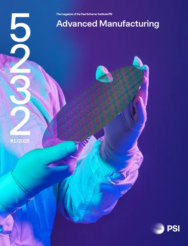
The research institute in Villigen has long been a well-known name in the semiconductor industry. “Over the years, almost all microchip manufacturers have come to PSI to carry out tests,” says Yasin Ekinci, head of the Laboratory for X-ray Nanoscience and Technologies, which is also part of the PSI Center for Photon Science. “In the semiconductor industry, advanced manufacturing means photolithography.” Ultraviolet light strikes a photomask, which serves as a template for the circuit paths and transistors on the chip. A complex optical system shrinks the image of this mask and projects it repeatedly onto a silicon layer coated with a photoresist.
“Initially, there were around 1,000 transistors on a chip; today, up to 100 billion transistors can fit on a chip the size of a thumbnail,” says Ekinci. This incredible miniaturisation has only been possible by switching to light with ever shorter wavelengths in photolithography. Today, the most powerful chips, such as those found in top-of-the-range smartphones, are made using extreme ultraviolet (EUV) light with a wavelength of 13.5 nanometres (1 nanometre is one millionth of a millimetre). This required a completely new technology, in the development of which PSI has played a major role.
The high-performance chips are manufactured using scanners that are probably the most complex machines ever built. Testing on the original devices would be risky as well as involving a huge amount of effort. So the industry takes advantage of the fact that the Swiss Light Source SLS too generates extreme ultraviolet light. “Here at the SLS we have a much simpler, faster and less expensive method for EUV lithography,” explains Ekinci. “Although we cannot use it to manufacture transistors, we can create extremely fine structures and offer a variety of testing options.” His team even holds a world record. While industrial “Over the years, almost all microchip manufacturers have come to PSI to carry out tests.” Yasin Ekinci, laboratory head at the PSI Center for Photon Science 5232 — #1/2025 13 Advanced Manufacturing EUV photolithography today produces structures with line widths of about ten nanometres, the finest patterns produced at SLS have a line width of just five nanometres. “These are the smallest structures ever made by humans,” says Ekinci.
In particular, a great many new potential photoresists have been tested at PSI. This is because the established materials are no longer suitable for EUV lithography. The tests carried out at PSI looked into whether a new photoresist was able to meet the requirements of the lithography process in terms of resolution and sensitivity. This collaboration with industry demands circumspection and confidentiality. Ekinci would have liked to develop a new photoresist himself, but for a long time he hesitated: “If we had done something similar to what our customers were doing, it might have been seen as a breach of trust,” he explains. “But now we have dared to try something completely new.”
Existing photoresists are based on polymers, which are large chains of molecules. “At the atomic level, they look like a bunch of cables,” says Ekinci. “If you want to write ever more finely, you need much smaller molecules as building blocks.” His group has therefore spent the last two years developing a new type of material based on a metal oxide. However, to convert this academic research into an industrial product will require large investments. That is why the PSI group is now working with the Finnish company PiBond, which has founded a subsidiary in Park Innovaare. PiBond will continue the development begun by PSI and commercialise it.

A skin for robots
Barbara Horvath’s newly founded spin-off company Inveel is also based at Park Innovaare. “Imagine a robot wanting to lift this coffee cup,” says the materials scientist, reaching for the cup on the table in front of her. “If its fingers were covered with the skin we are developing, it would be able to do this very easily.” Horvath has been awarded a Founder Fellowship by PSI, to help her turn her research results into an actual product.
As a postdoctoral researcher at PSI, Horvath developed a new manufacturing method for printing electronic circuits directly onto a polymer surface “at very high resolution, very quickly and covering large areas,” she explains. She and her team are now working on a prototype of robot skin. Tiny sensors are printed in close proximity to each other on a largearea film, on a scale down to just a few hundred nanometres. “If you apply this skin to a robot’s fingertips, it can not only feel individual points, but also assemble them to form a kind of tactile map that tells it whether it is touching the top, bottom or the middle of an object,” explains Horvath. “This allows it to grip and handle the object much better.”
Horvath’s process begins with the design and manufacture of a precise stamp. This takes place in PSI’s newly built, 450-square-metre cleanroom at Park Innovaare. “Here we have the necessary hightech machines and excellent conditions,” she says. The stamp is brought into contact with the material to prepare the surface. This enables the precise placement of metallic nanoparticles in the next step. These in turn are finally fused into tiny nanowires. Horvath does not want to reveal any further details: “We are still applying for patents, and I do not want to jeopardise this process.”
If you apply this skin to a robot’s fingertips, it can not only feel individual points, but also assemble them to form a kind of tactile map.
The manufacturing process could be used for many other applications, such as smart windows that only allow certain wavelengths of incident light to pass through, thereby regulating the temperature. But for now, Horvath wants to concentrate on getting the robot skin ready for the market. Temperature and humidity sensors could also be printed onto the polymer surface. This would allow a robot to sense when someone is breathing nearby. “At the moment, that sounds very futuristic,” she admits. But she is convinced that this development will assert itself: “A robot like this could soon pick up my cup and return it.”