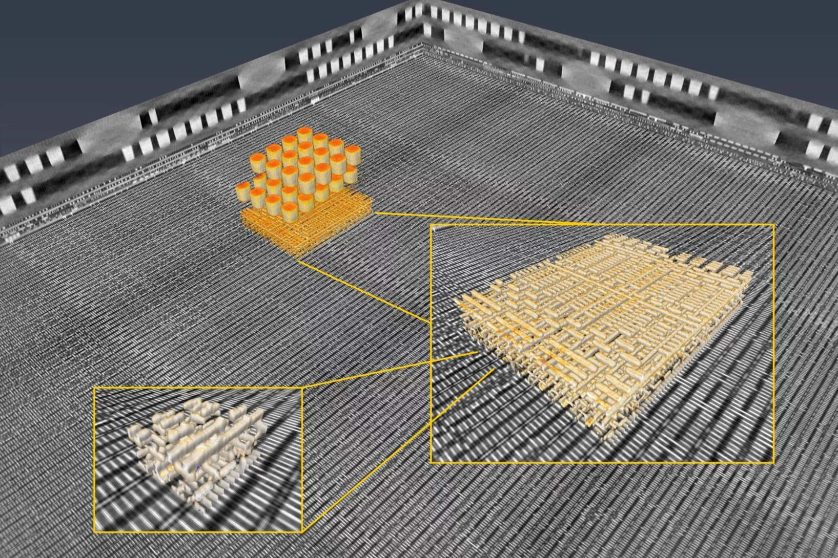
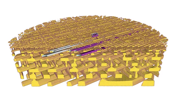
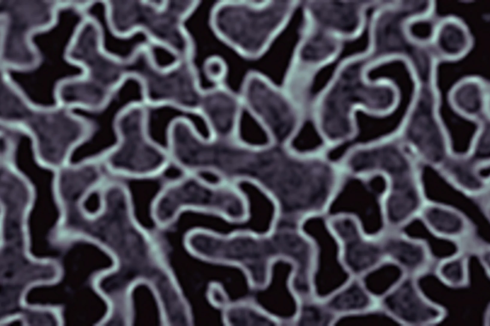
In a collaboration with EPFL Lausanne, ETH Zurich and the University of Southern California researchers at the Paul Scherrer Institute PSI have used X-rays to look inside a microchip with higher precision than ever before. The image resolution of 4 nanometres marks a new world record. The high-resolution three-dimensional images of the type they produced will enable advances in both information technology and the life sciences. The researchers are reporting their findings in the current issue of the journal Nature.
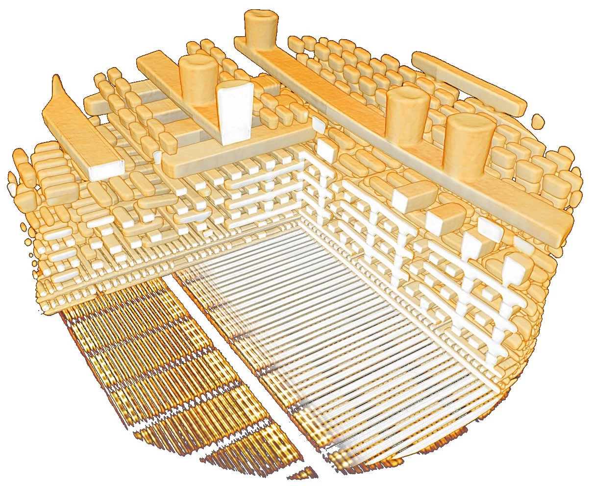
Since 2010, the scientists at the Laboratory of Macromolecules and Bioimaging at PSI have been developing microscopy methods with the goal of producing three-dimensional images in the nanometre range. In their current research, a collaboration with the EPFL and the ETHZ, the Swiss Federal Institutes of Technology in Lausanne and Zürich, and the University of Southern California, they have succeeded for the first time in taking pictures of state-of-the-art computer chips microchips with a resolution of 4 nanometres, i.e. 4 millionths of a millimetre – a world record. Instead of using lenses, with which images in this range are not currently possible, the scientists resort to a technique known as ptychography, in which a computer combines many individual images to create a single, high-resolution picture. Shorter exposure times and an optimised algorithm were key to significantly improving upon the world record they themselves set in 2017. For their experiments, the researchers used X-rays from the Swiss Light Source SLS at PSI.
Between conventional X-ray tomography and electron microscopy
Microchips are marvels of technology. Nowadays, it is possible to pack more than 100 million transistors per square millimetre into advanced integrated circuits – a trend that continues to increase. Highly automated optical systems are used to etch the nanometre-sized circuit traces into silicon blanks in clean rooms. Layer after layer is added and removed until the finished chip, the brains of our smartphones and computers, can be cut out and installed. The manufacturing process is elaborate and complicated, and characterising and mapping the resulting structures proves to be just as difficult.
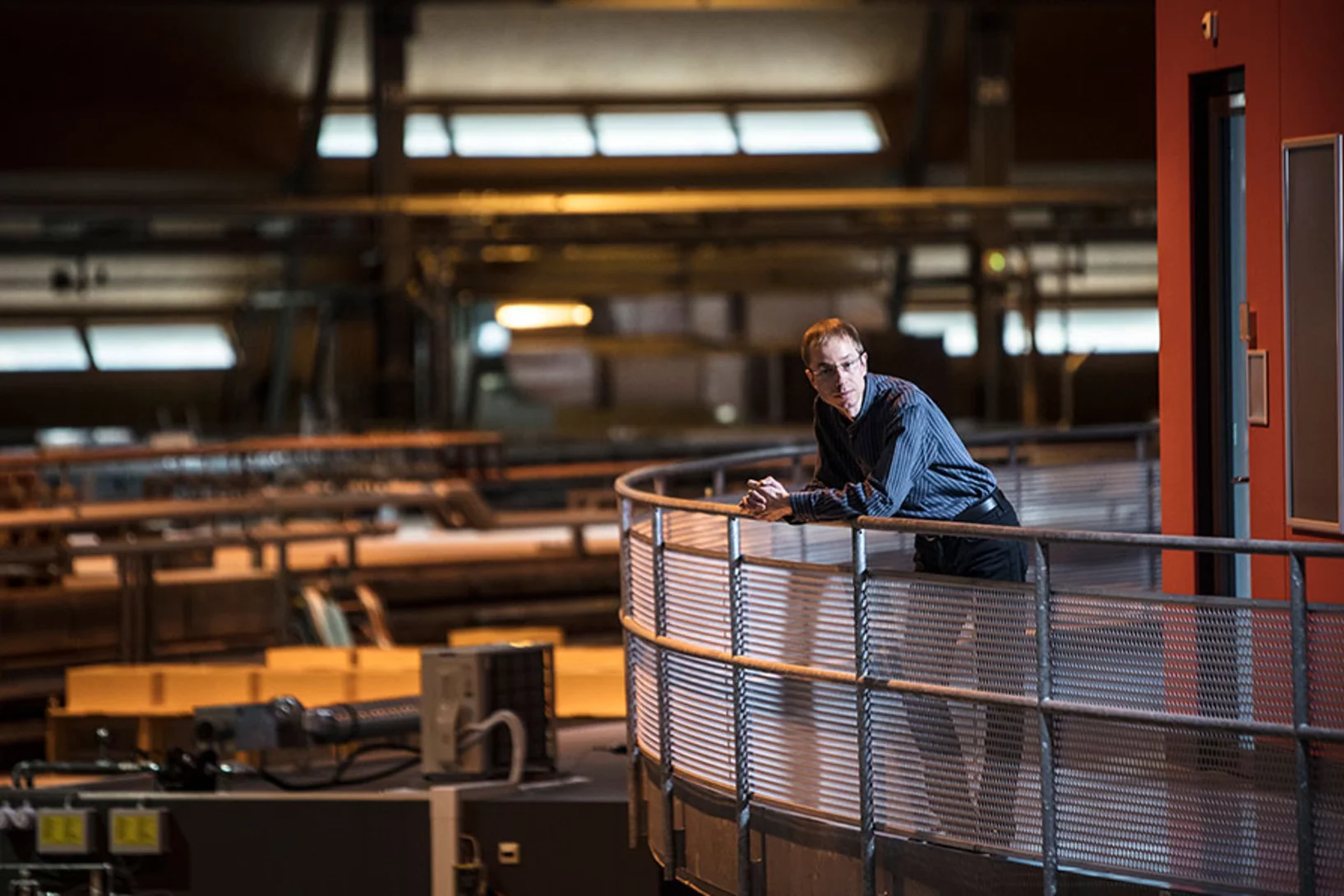
While scanning electron microscopes have a resolution of a few nanometres and are therefore well suited to imaging the tiny transistors and metal interconnects that make up circuits, they can only produce two-dimensional images of the surface. “The electrons don’t travel far enough into the material,” explains Mirko Holler, a physicist at SLS. “To construct three-dimensional images with this technique, the chip has to be examined layer by layer, removing individual layers at the nanometre level – a very complex and delicate process which also destroys the chip.”
However, three-dimensional and non-destructive images can be produced using X-ray tomography, because X-rays can penetrate materials much further. This procedure is similar to a CT scan in a hospital. The sample is rotated and X-rayed from different angles. The way the radiation is absorbed and scattered varies, depending on the internal structure of the sample. A detector records the light leaving the sample and an algorithm reconstructs the final 3D image from it. “Here we have a problem with the resolution,” explains Mirko Holler. “None of the X-ray lenses currently available can focus this radiation in a way that allows such tiny structures to be resolved.”
Ptychography – the virtual lens
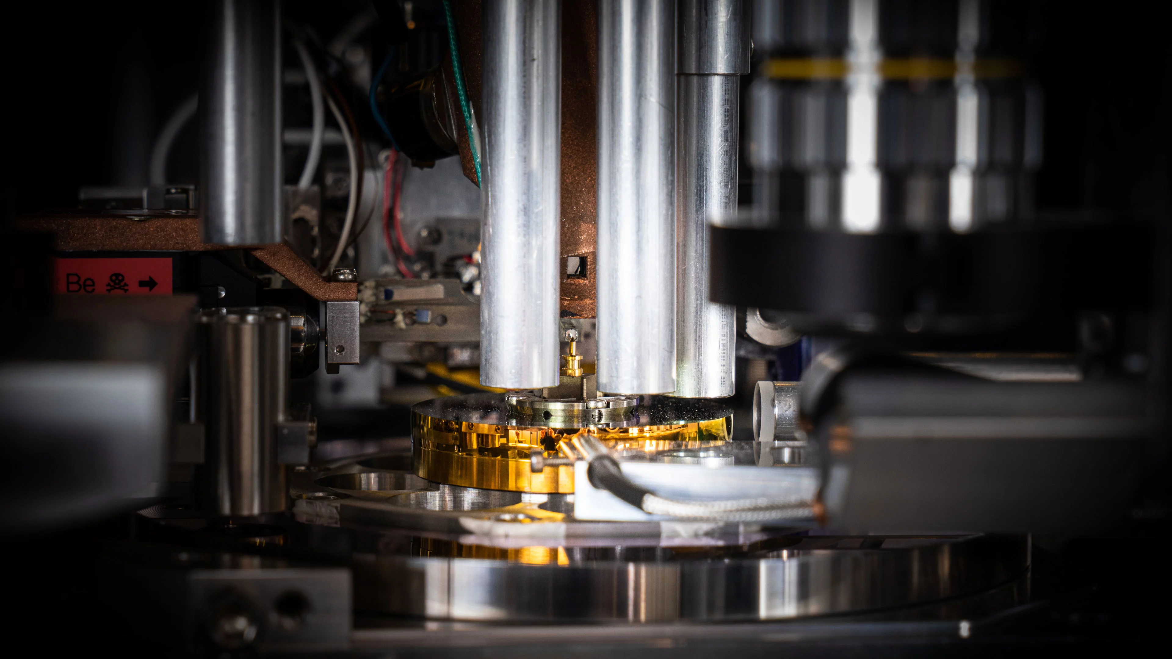
The solution is ptychography. In this technique, the X-ray beam is not focused on a nanometre scale; instead, the sample is moved on a nanometre scale. “Our sample is moved such that the beam follows a precisely defined grid – like a sieve. At each point along the grid, a diffraction pattern is recorded,” explains the physicist. The distance between the individual grid points is less than the diameter of the beam, so the imaged areas overlap. This produces enough information to reconstruct the sample image at a high resolution with the help of an algorithm. The reconstruction process is rather like using a virtual lens.
“Since 2010, we have been steadily perfecting our experimental set-up and the accuracy with which we position our samples. In 2017, we finally succeeded in spatially imaging a computer chip with a resolution of 15 nanometres – a record,” Holler recalls. Since then, the resolution has remained unchanged in our instrument, despite further optimisations in the set-up and the algorithm. “We extended it by one or two nanometres, but that was as far as we could go. Something was limiting us and we had to find out what it was.”
The search for the limiting factor
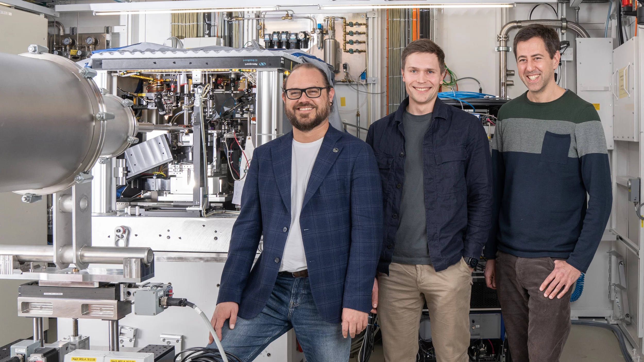
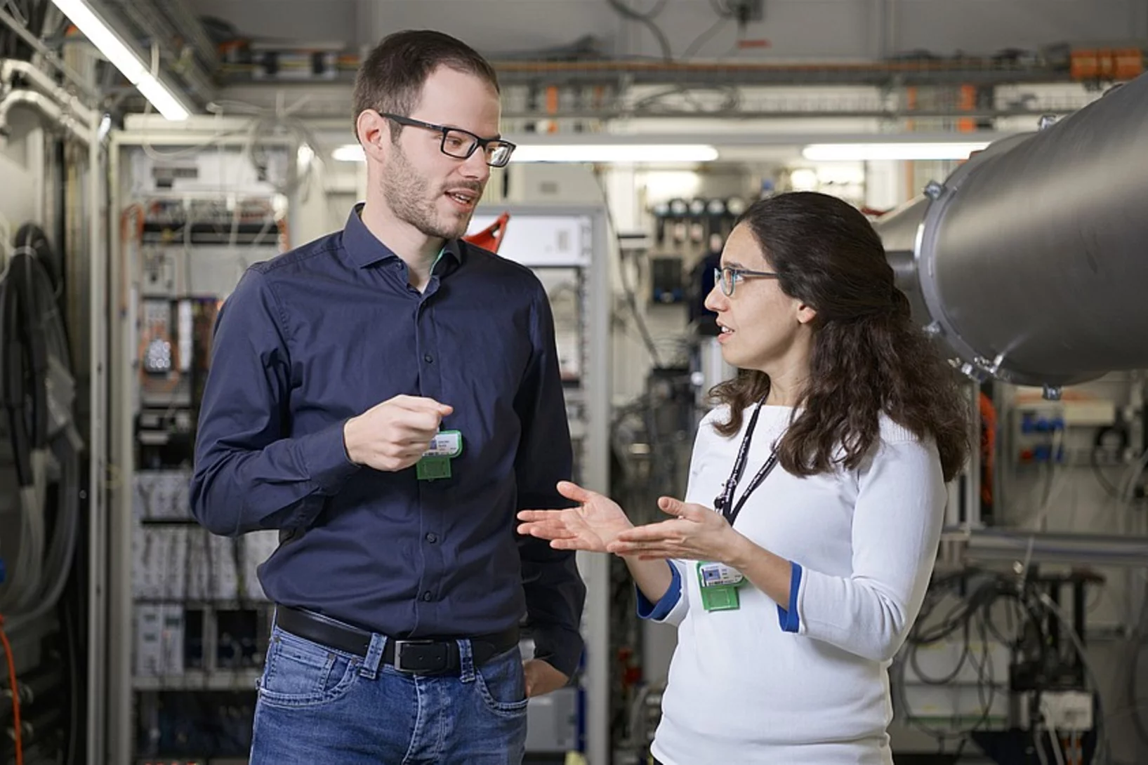
The elaborate search finally began in 2021 with a project funded by the Swiss National Science Foundation. In addition to Mirko Holler and Manuel Guizar-Sicairos, who had both been involved in the first record, Tomas Aidukas also joined the group. The physicist supported the team with his programming experience and developed the new algorithm which ultimately helped them to achieve the breakthrough.
The researchers found their first clue when they reduced the exposure time – suddenly the diffraction images were sharper. This led them to conclude that the X-ray beam illuminating the sample was not stable, but instead moving by tiny amounts – the beam was wobbling. “This is analogous to photography,” Guizar-Sicairos explains. “When you take a picture at night, you choose a long exposure because of the darkness. If you do this without using a tripod, your movements are transmitted to the camera and the picture will be blurred.” On the other hand, if you choose a short exposure time so that the light is captured faster than we move, then the image will be sharp. “But in that case, the picture might be completely black or noisy, because almost no light can be captured in that short amount of time.”
The researchers faced a similar problem. Although their images were now sharp, they contained too little information to reconstruct the entire microchip, because of the short exposure time.
Shorter exposure time and a new algorithm
To solve the problem, the researchers upgraded their set-up with a faster detector, also developed at PSI. This allowed them to record many images at each grid point, each with a short exposure time. “A huge mountain of data,” Aidukas adds. When the individual images are added together and superimposed, this results in the same blurry image that was obtained using a long exposure time.
“You can think of the X-ray beam as one point on the sample. We now take a whole lot of individual pictures at this particular point,” explains Aidukas. Since the beam is wobbling, each image will change slightly. “In some of the pictures, the beam is in the same position, in others it has moved. We can use these changes to track the actual position of the beam caused by the unknown vibrations.” The next thing is to reduce the amount of data. “Our algorithm compares the positions of the beam in the individual images. If the positions are the same, they are put in the same group and added to the sum.” By grouping the low-exposure images, their information content can be increased. As a result, the researchers are able to reconstruct a sharp image with a high light content using the flood of short-exposure pictures.
The new ptychographic technique is a basic approach that can also be used at similar research facilities. The method is not confined to microchips, but can also be used on other samples, for example in materials science or life sciences.
About PSI
The Paul Scherrer Institute PSI develops, builds and operates large, complex research facilities and makes them available to the national and international research community. The institute's own key research priorities are in the fields of future technologies, energy and climate, health innovation and fundamentals of nature. PSI is committed to the training of future generations. Therefore about one quarter of our staff are post-docs, post-graduates or apprentices. Altogether PSI employs 2300 people, thus being the largest research institute in Switzerland. The annual budget amounts to approximately CHF 450 million. PSI is part of the ETH Domain, with the other members being the two Swiss Federal Institutes of Technology, ETH Zurich and EPFL Lausanne, as well as Eawag (Swiss Federal Institute of Aquatic Science and Technology), Empa (Swiss Federal Laboratories for Materials Science and Technology) and WSL (Swiss Federal Institute for Forest, Snow and Landscape Research). (Last updated in June 2025)
Contact
Original Publication
-
Aidukas T, Phillips NW, Diaz A, Poghosyan E, Müller E, Levi AFJ, et al.
High-performance 4-nm-resolution X-ray tomography using burst ptychography
Nature. 2024; 632(8023): 81-88. https://doi.org/10.1038/s41586-024-07615-6
DORA PSI
