A novel super-resolution X-ray microscope developed by a team of researchers from the Paul Scherrer Institut (PSI) and EPFL in Switzerland combines the high penetration power of x-rays with high spatial resolution, making it possible for the first time to shed light on the detailed interior composition of semiconductor devices and cellular structures.
The first super-resolution images from this novel microscope will be published online July 18, 2008 in the journal Science.
Researchers have been working on such super-resolution microscopy concepts for electrons and x-rays for many years,
says EPFL Professor and team leader Franz Pfeiffer. Only the construction of a dedicated multi-million Swiss-franc instrument at PSI's Swiss Light Source allowed us to achieve the stability that is necessary to implement our novel method in practice.
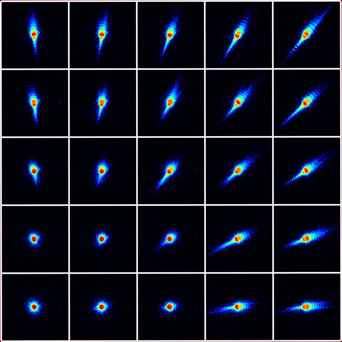
The new instrument uses a Megapixel Pilatus detector (whose big brother will be detecting collisions from CERN's Large Hadron Collider), which has excited the synchrotron community for its ability to count millions of single x-ray photons over a large area. This key feature makes it possible to record detailed diffraction patterns while the sample is raster-scanned through the focal spot of the beam. In contrast, conventional x-ray (or electron) scanning microscopes measure only the total transmitted intensity.
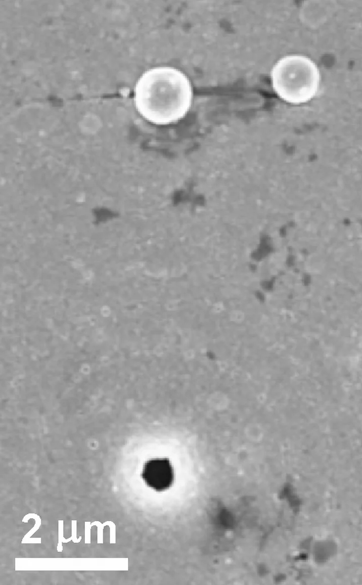
These diffraction data are then treated with an algorithm conceived by the Swiss team. We developed an image reconstruction algorithm that deals with the several tens of thousands of diffraction images and combines them into one super-resolution x-ray micrograph,
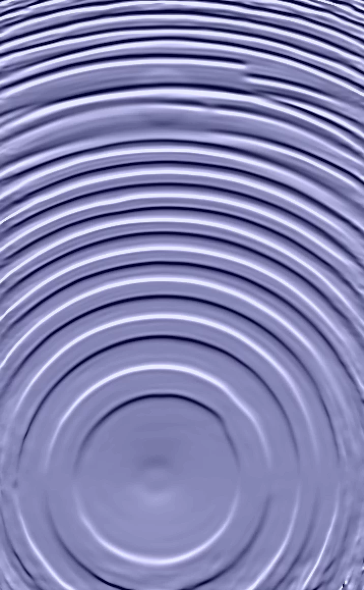
explains PSI researcher Pierre Thibault, first author on the publication. In order to achieve images of the highest precision, the algorithm not only reconstruct the sample but also the exact shape of the light probe resulting from the x-ray beam.
Conventional electron scanning microscopes can provide high-resolution images, but usually only for the surface of the specimen, and the samples must be kept in vacuum. The Swiss team's new super-resolution microscope bypasses these requirements, meaning that scientists will now be able to look deeply into semiconductors or biological samples without altering them. It can be used to non-destructively characterize nanometer defects in buried semiconductor devices and to help improve the production and performance of future semiconductor devices with sub-hundred-nanometer features. A further very promising application of the technique is in high-resolution life science microscopy, where the penetration power of X-rays can be used to investigate embedded cells or sub-cellular structures. Finally, the approach can also be transferred to electron or visible laser light, and help in the design of new and better light and electron microscopes.
Contact
Reference
High-Resolution Scanning X-Ray Diffraction Microscopy, by P. Thibault et al., Science, Vol 321 (2008).
About PSI
The Paul Scherrer Institute PSI develops, builds and operates large, complex research facilities and makes them available to the national and international research community. The institute's own key research priorities are in the fields of future technologies, energy and climate, health innovation and fundamentals of nature. PSI is committed to the training of future generations. Therefore about one quarter of our staff are post-docs, post-graduates or apprentices. Altogether PSI employs 2300 people, thus being the largest research institute in Switzerland. The annual budget amounts to approximately CHF 450 million. PSI is part of the ETH Domain, with the other members being the two Swiss Federal Institutes of Technology, ETH Zurich and EPFL Lausanne, as well as Eawag (Swiss Federal Institute of Aquatic Science and Technology), Empa (Swiss Federal Laboratories for Materials Science and Technology) and WSL (Swiss Federal Institute for Forest, Snow and Landscape Research). (Last updated in June 2025)


