
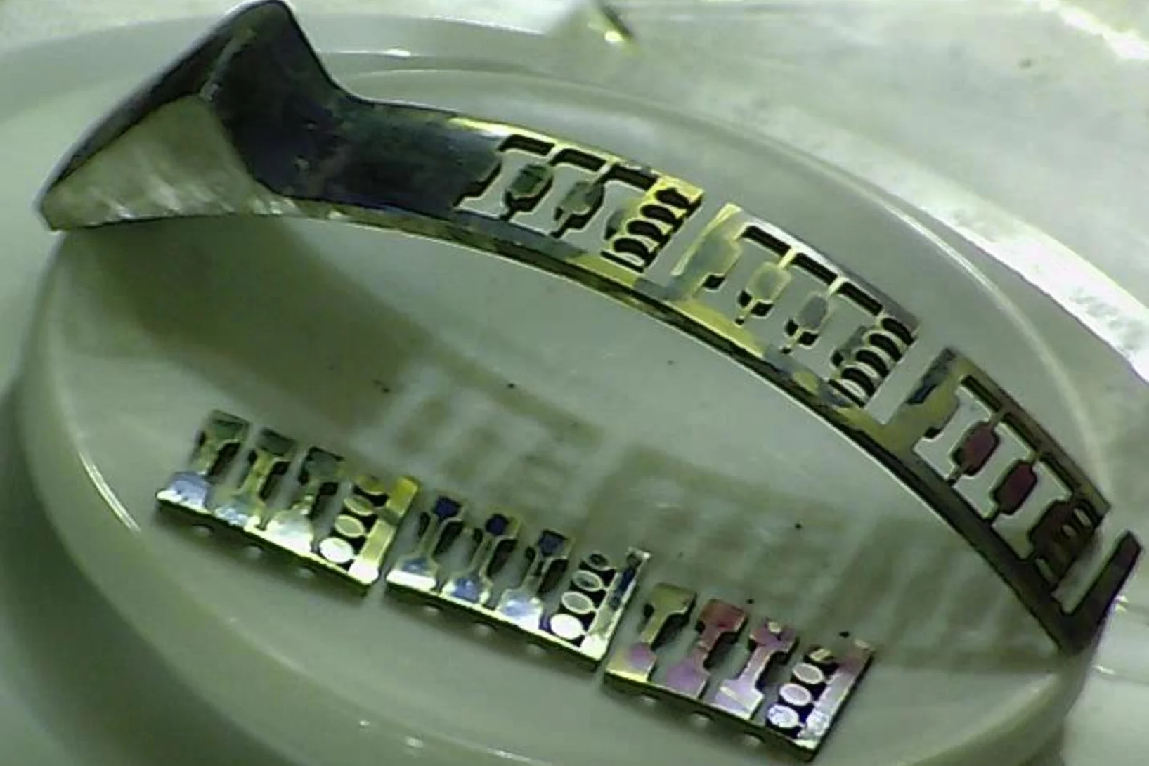
MEGAPIE samples delivered to partners for post irradiation investigation
The MEGAWatt Pilot Experiment was operated for neutron generation with the PSI high intensity proton beam in 2006. The experiment utilized liquid target material, a lead bismuth eutectic. This marked a major milestone towards Accelerator Driven Systems (ADS), which are intended to be used for the incineration of nuclear waste.

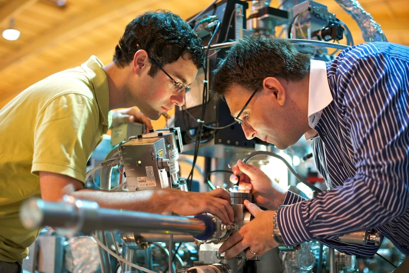
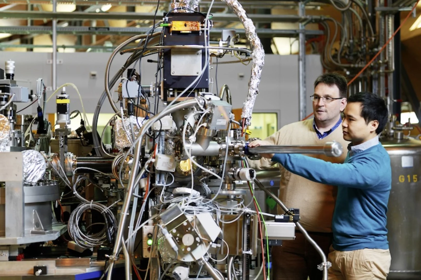
Tiny Magnets as a Model System
Scientists use nano-rods to investigate how matter assembles
In the microscopic world, everything is in motion: atoms and molecules vibrate, proteins fold, even glass is a slow flowing liquid. And during each movement there are interactions between the smallest elements - for example, the atoms - and their neighbours. To make these movements visible, scientists at the Paul Scherrer Institute PSI have developed a special model system.
Atomic motions untangled
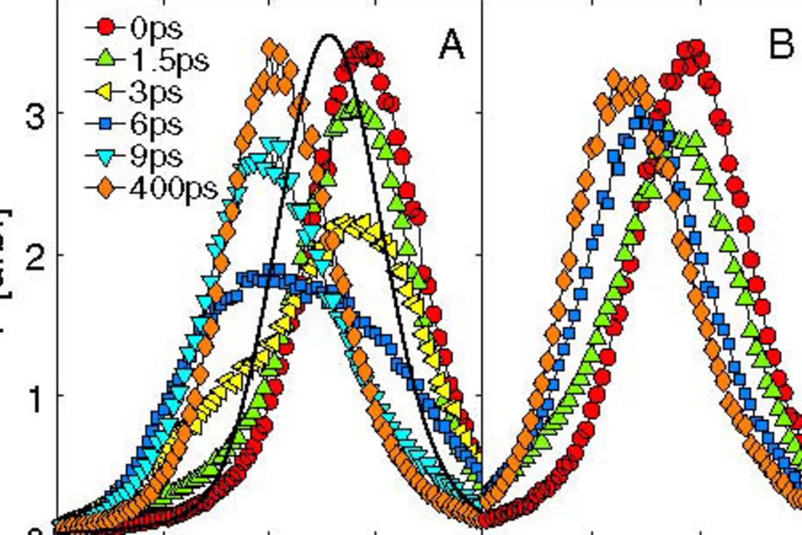
The pursuit of capturing motion in a movie bears an obvious fascination irrespective of the time scales involved. In the atomic and molecular world where the masses are so light and the distances small the relevant time scale shifts to the subpicosecond range and the motions become frantic especially for larger molecular systems.
Atomic motions untangled
The pursuit of capturing motion in a movie bears an obvious fascination irrespective of the time scales involved. In the atomic and molecular world where the masses are so light and the distances small the relevant time scale shifts to the ubpicosecond range and the motions become frantic especially for larger molecular systems
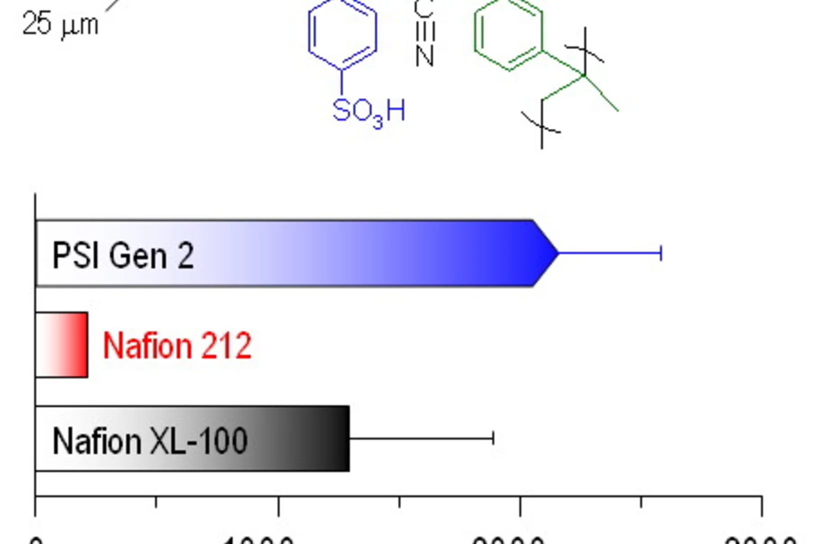
Radiation grafted membranes developed at PSI outlast state-of-the art commercial membranes in the fuel cell
Components for the polymer electrolyte fuel cell (PEFC) are required to show high performance and durability under application relevant conditions. Furthermore, for commercial viability the materials and processes for component fabrication need to be of los cost. The polymer electrolyte membrane developed at PSI on the basis of the radiation grafting technique has the potential of being produced in cost-effective manner. In recent years, we have collaborated with the Belenos Clean Power to further develop the membrane to commercial competitiveness.

On Proton Conductivity in Porous and Dense Yttria Stabilized Zirconia at Low Temperature
The electrical conductivity of dense and nanoporous zirconia-based thin films is compared to results obtained on bulk yttria stabilized zirconia (YSZ) ceramics. Different thin film preparation methods are used in order to vary grain size, grain shape, and porosity of the thin films. In porous films, a rather high conductivity is found at room temperature which decreases with increasing temperature to 120 °C. This conductivity is attributed to proton conduction along physisorbed water (Grotthuss mechanism) at the inner surfaces.
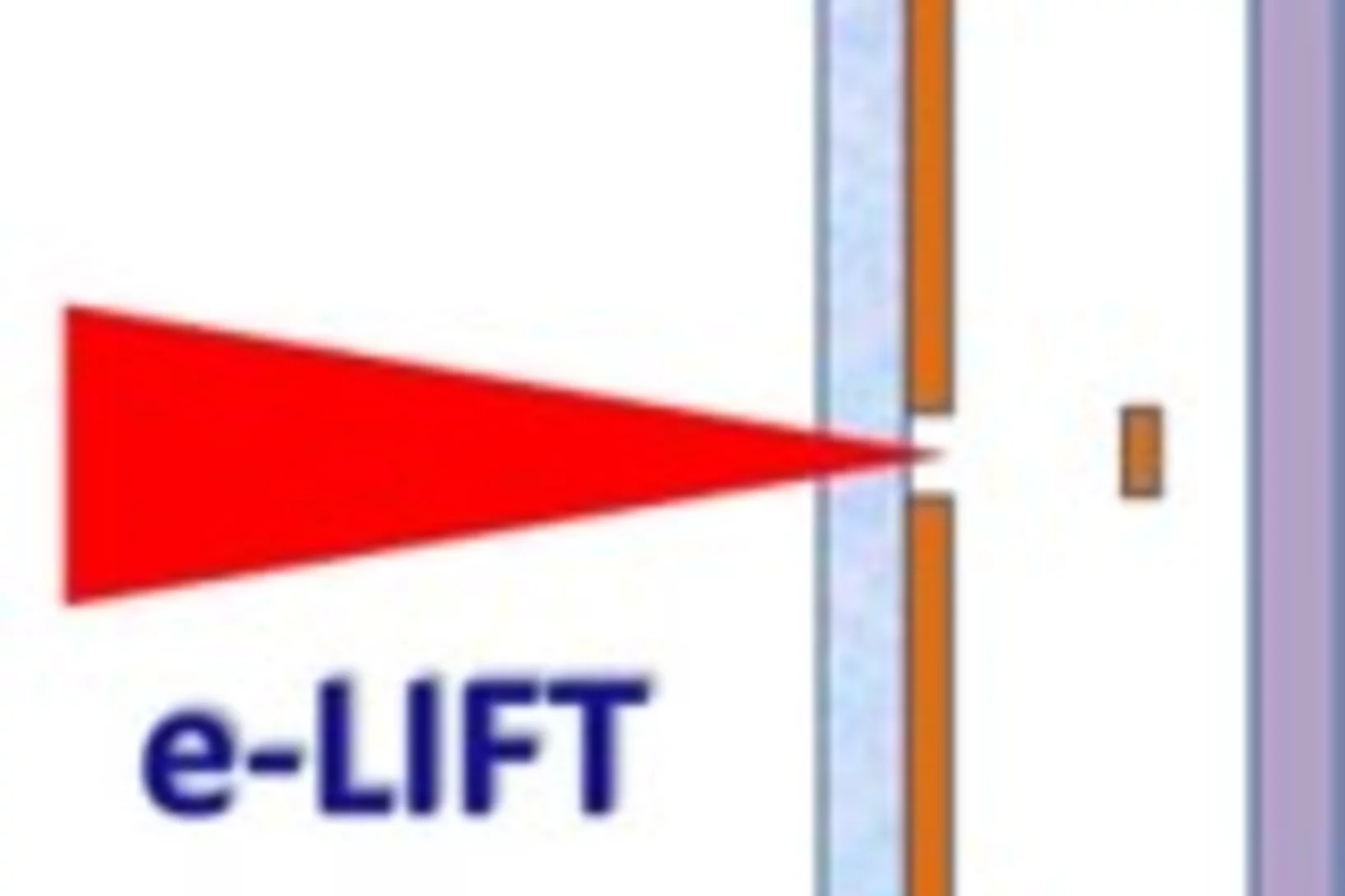
Applications of laser printing for organic electronics
The development of organic electronic requires a non contact digital printing process. The European funded e-LIFT project investigated the possibility of using the Laser Induced Forward Transfer (LIFT) technique to address this field of applications. This process has been optimized for the deposition of functional organic and inorganic materials in liquid and solid phase, and a set of polymer dynamic release layer (DRL) has been developed to allow a safe transfer of a large range of thin films.
Electric-Field-Induced Polar Order and Localization of the Confined Electrons in LaAlO3/SrTiO3 Heterostructures
With ellipsometry, x-ray diffraction, and resistance measurements we investigated the electric-field effect on the confined electrons at the LaAlO3/SrTiO3 interface. We obtained evidence that the localization of the electrons at negative gate voltage is induced, or at least enhanced, by a polar phase transition in SrTiO3 which strongly reduces the lattice polarizability and the subsequent screening. In particular, we show that the charge localization and the polar order of SrTiO3 both develop below ∼50 K and exhibit similar, unipolar hysteresis loops as a function of the gate voltage.
Soft x-ray photoelectron spectroscopy on buried complex oxide interfaces: a new method to diagnose authentic protected electronic structures
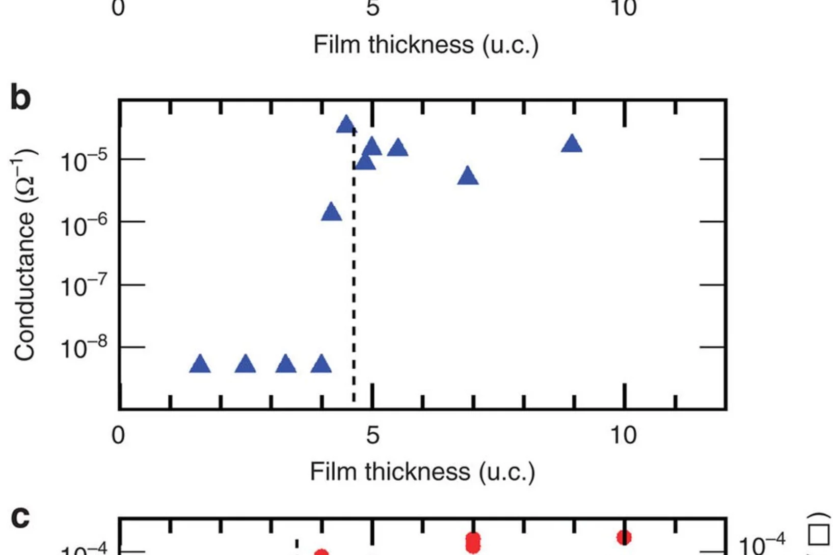
Exotic phenomena at interfaces of complex oxides are highly promising for future solid-state electronics applications. A prominent example is the interface of two wide band gap insulators formed by growing a LaAlO3 layer on TiO2-terminated SrTiO3 substrate. When the LaAlO3 thickness exceeds 3 unit cells this system undergoes a sharp insulator-to-metal transition with a two-dimensional electron gas (2DEG) appearing at the interface.
Magnetic Cluster Excitations
Magnetic clusters, i.e., assemblies of a finite number (between two or three and several hundred) of interacting spin centers which are magnetically decoupled from their environment, can be found in many materials ranging from inorganic compounds and magnetic molecules to artificial metal structures formed on surfaces and metalloproteins.
Imaging fluctuations with X-ray microscopy
X-rays allow an inside look at structures that cannot be imaged using visible light. They are used to investigate nanoscale structures of objects as varied as single cells or magnetic storage media. Yet, high-resolution images impose extreme constraints on both the X ray microscope and the samples under investigation.
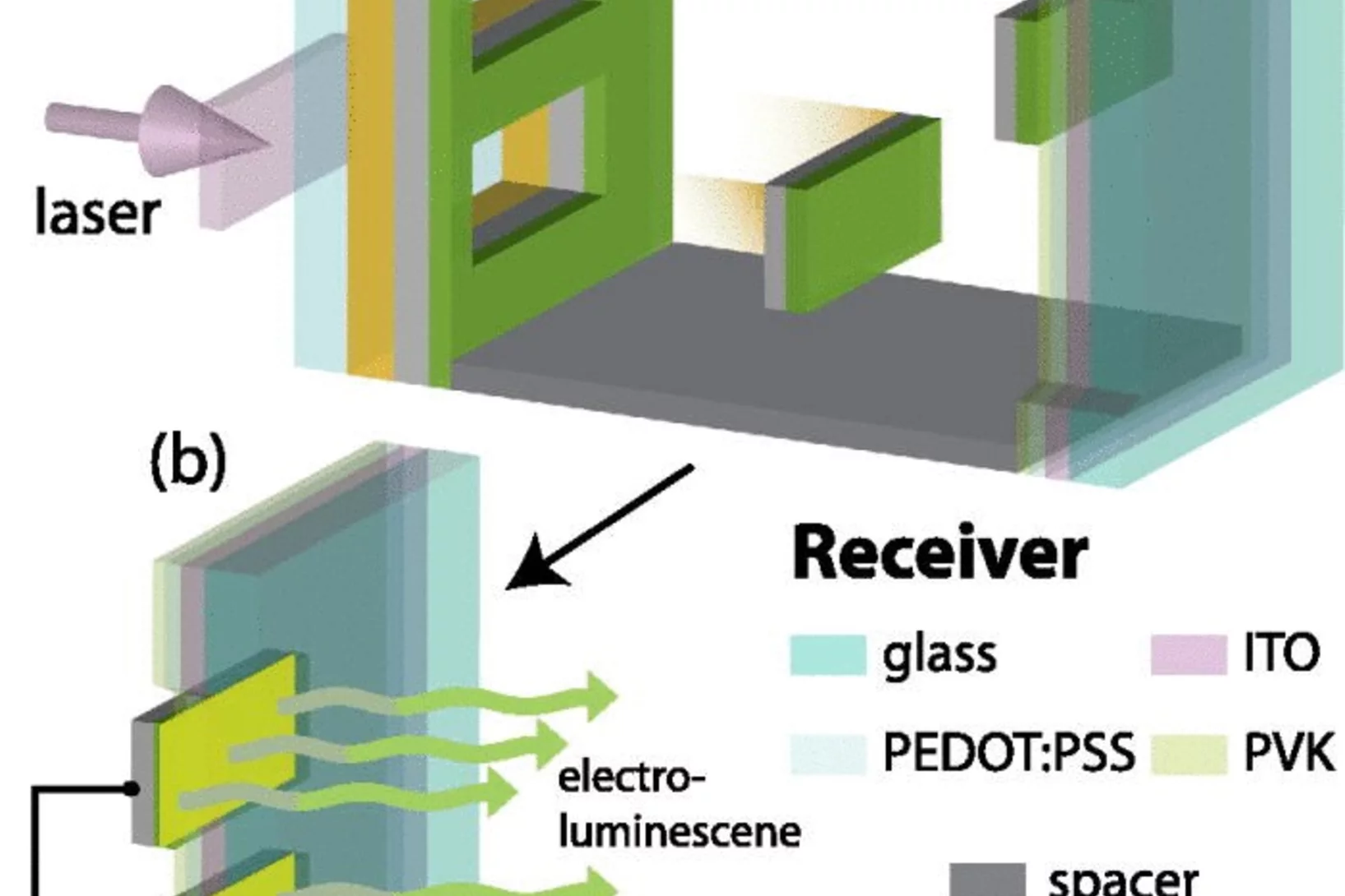
The fabrication of small molecule organic light-emitting diode pixels by laser-induced forward transfer
Laser-induced forward transfer (LIFT) is a versatile organic light-emitting diode (OLED) pixel deposition process, but has hitherto been applied exclusively to polymeric materials. Here, a modified LIFT process has been used to fabricate small molecule Alq3 organic light-emitting diodes (SMOLEDs). Small molecule thin films are considerably more mechanically brittle than polymeric thin films, which posed significant challenges for LIFT of these materials.
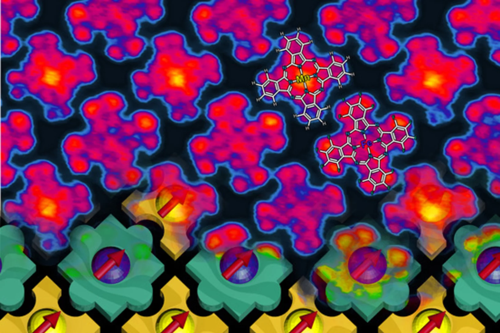
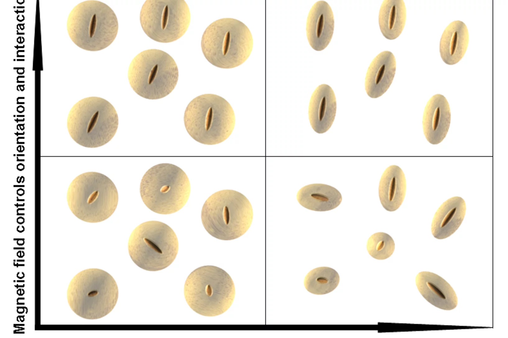
Magnetic nano-chessboard puts itself together
Researchers from the Paul Scherrer Institute and the Indian Institute of Science Education and Research (Pune, India) have managed to ‘turn off’ the magnetization of every second molecule in an array of magnetized molecules and thereby create a ‘magnetic chessboard’. The magnetic molecules were so constructed that they were able to find their places in the nano-chessboard by themselves.
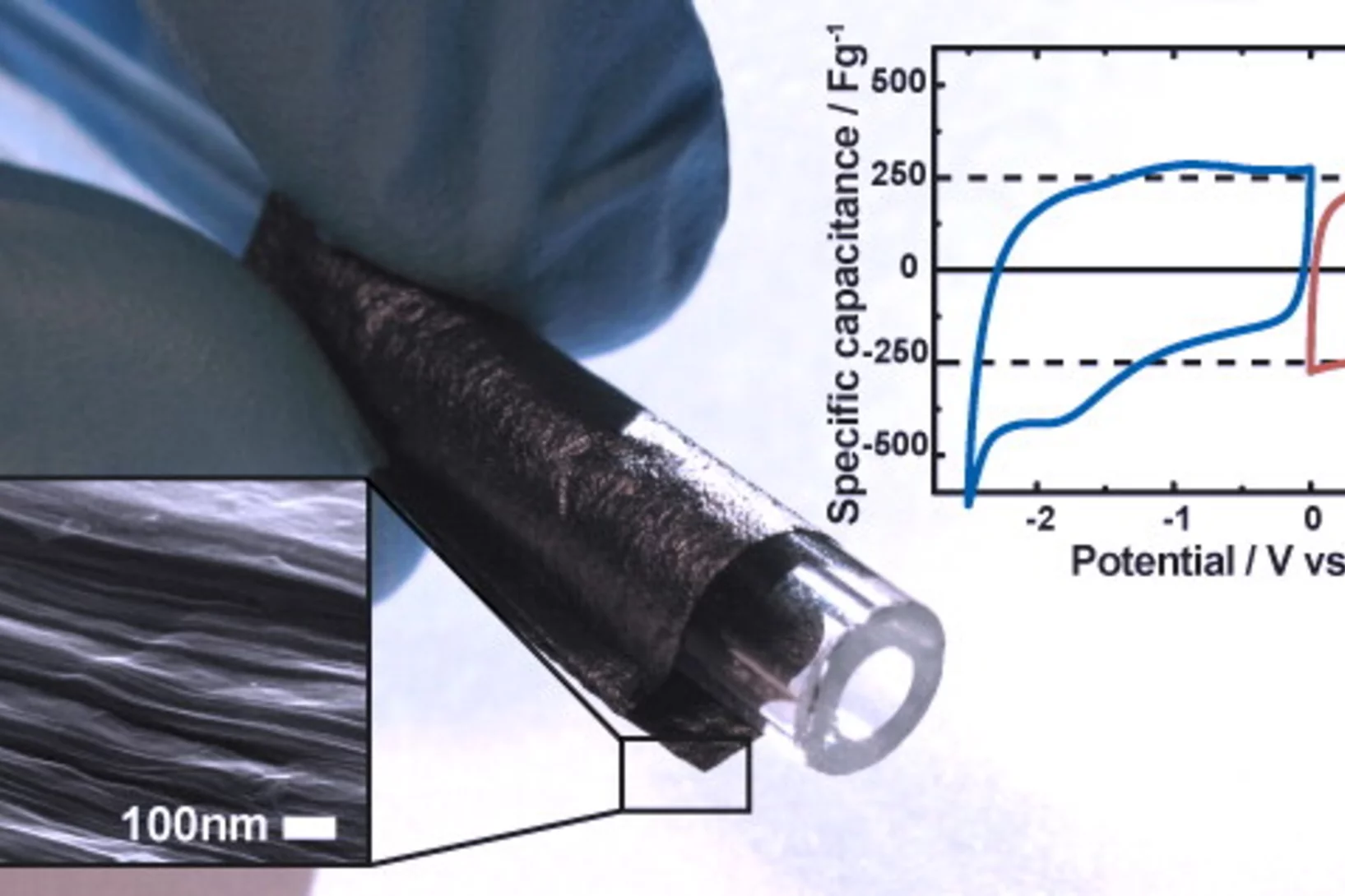
Partially reduced graphene oxide paper: a thin film electrode for electrochemical capacitors
One way to utilize graphene and its’ outstanding specific surface area of 2630 m2g-1 for supercapacitor electrodes is by preparing a so called free-standing graphene paper. Such a flexible, conductive graphene-paper electrode was prepared by a flow-directed filtration of graphene oxide dispersion followed by a gentle thermal reduction treatment of the filtrate. The prepared partially reduced graphene oxide paper (GOPpr) showed a dense packing of graphene sheets with a distinct interlayer distance of 4.35 Å.
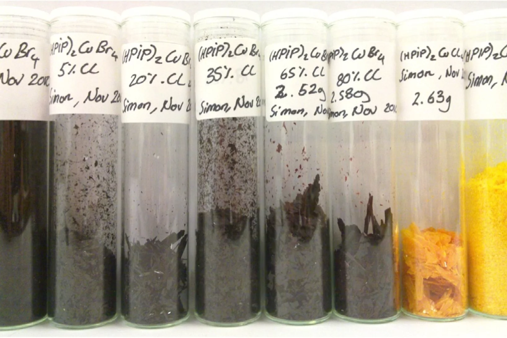
Spin ladders and quantum simulators for Tomonaga-Luttinger liquids
Magnetic insulators have proven to be usable as quantum simulators for itinerant interacting quantum systems. In particular the compound (C5H12N)2CuBr4 (for short: (Hpip)2CuBr4) was shown to be a remarkable realization of a Tomonaga-Luttinger liquid (TLL) and allowed us to quantitatively test the TLL theory.
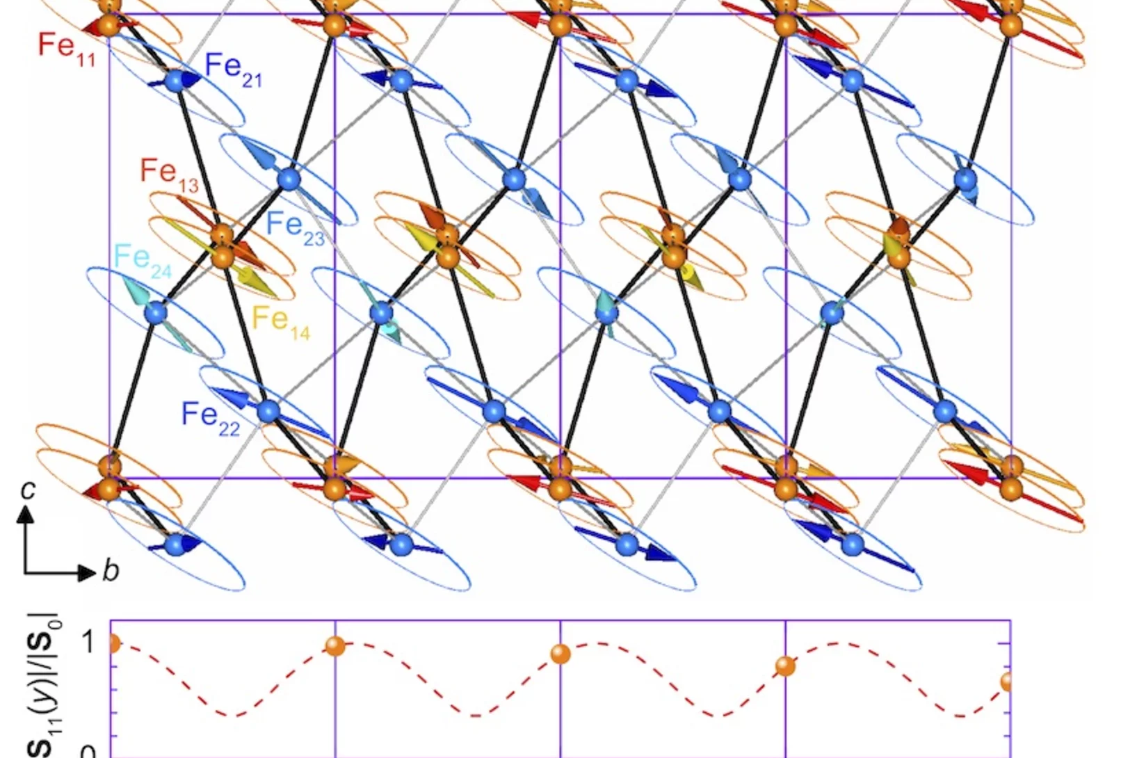
Persistent Spin Dynamics Intrinsic to Amplitude-Modulated Long-Range Magnetic Order
In geometrically and/or exchange frustrated materials spin fluctuations may endure down to lowest accessible temperatures - the phenomenon known as persistent spin dynamics. Since spin fluctuations hinder the onset of extended static correlations, persistent spin dynamics and long-range magnetic order are generally considered as mutually exclusive. Remarkably, their coexistence has been found in several frustrated magnetic systems but was lacking a suitable explanation.
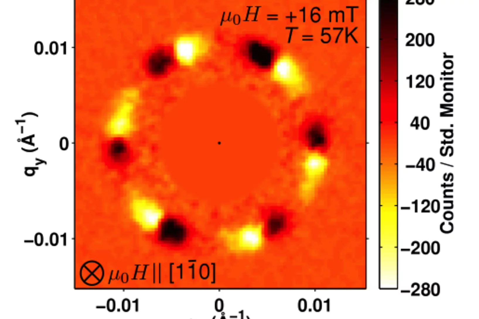
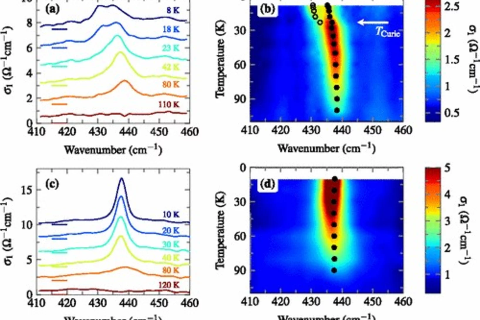
Electric field control of the skyrmion lattice in Cu2OSeO3
Skyrmions are topologically protected magnetic spin 'whirls' that form a hexagonal 2D lattice in non-centrosymmetric magnets. Until recently, skyrmions had only been observed in itinerant metallic alloys such as MnSi, where they can also be manipulated by applied electric currents.
X-rays provide insights into volcanic processes
Experiments performed at the Paul Scherrer Institute (PSI) investigate processes inside volcanic materials that determine whether a volcano will erupt violently or mildly.
New Insights into Superconducting Materials
An American-Swiss research team has used a new X-ray technique at Swiss Light Source (SLS) of the Paul Scherrer Institute (PSI) to investigate the magnetic properties of atomically thin layers of a parent compound of a high-temperature superconductor. It turns out that the magnetic properties of such thin films differ by only a surprisingly small degree from those of macroscopically thick samples.
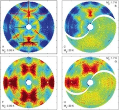
Power-Law Spin Correlations in the Pyrochlore Antiferromagnet Tb2Ti2O7
Spin correlations with power-law decay are usually associated with a critical point, but stable phases with power-law correlations may exist in frustrated magnets. Such phases are interesting, because they represent model materials where short-range interactions and local constraints lead to emergent symmetries and fractional quasiparticles.
ERC Grant for the development of a new imaging method with high potential clinical impact
Marco Stampanoni, Assistant Professor for X-ray microscopy at the ETH Zürich and Head of the 'X-ray Tomography Group' of the SLS has been recently awarded one of the coveted European Research Council (ERC) Starting Grant for the project PhaseX: 'Phase contrast X-ray imaging for medicine'. Marco Stampanoni's project will be supported by the ERC with 1.5 million euros for the next 5 years. The highly competitive ERC Starting Grants are reserved for outstanding young research talents.
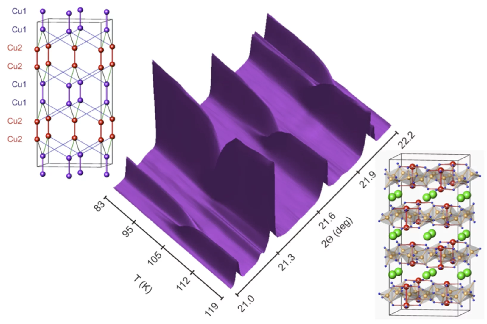
Two types of adjacent dimer layers in the low temperature phase of BaCuSi2O6
The interest in BaCuSi2O6 is motivated by its extraordinary phase diagram with field-induced Bose-Einstein condensation. Being a quantum paramagnet at zero magnetic field down to the lowest temperatures, the system displays a quantum phase transition into a magnetically ordered state at the critical value of magnetic field of ~23.5 T.
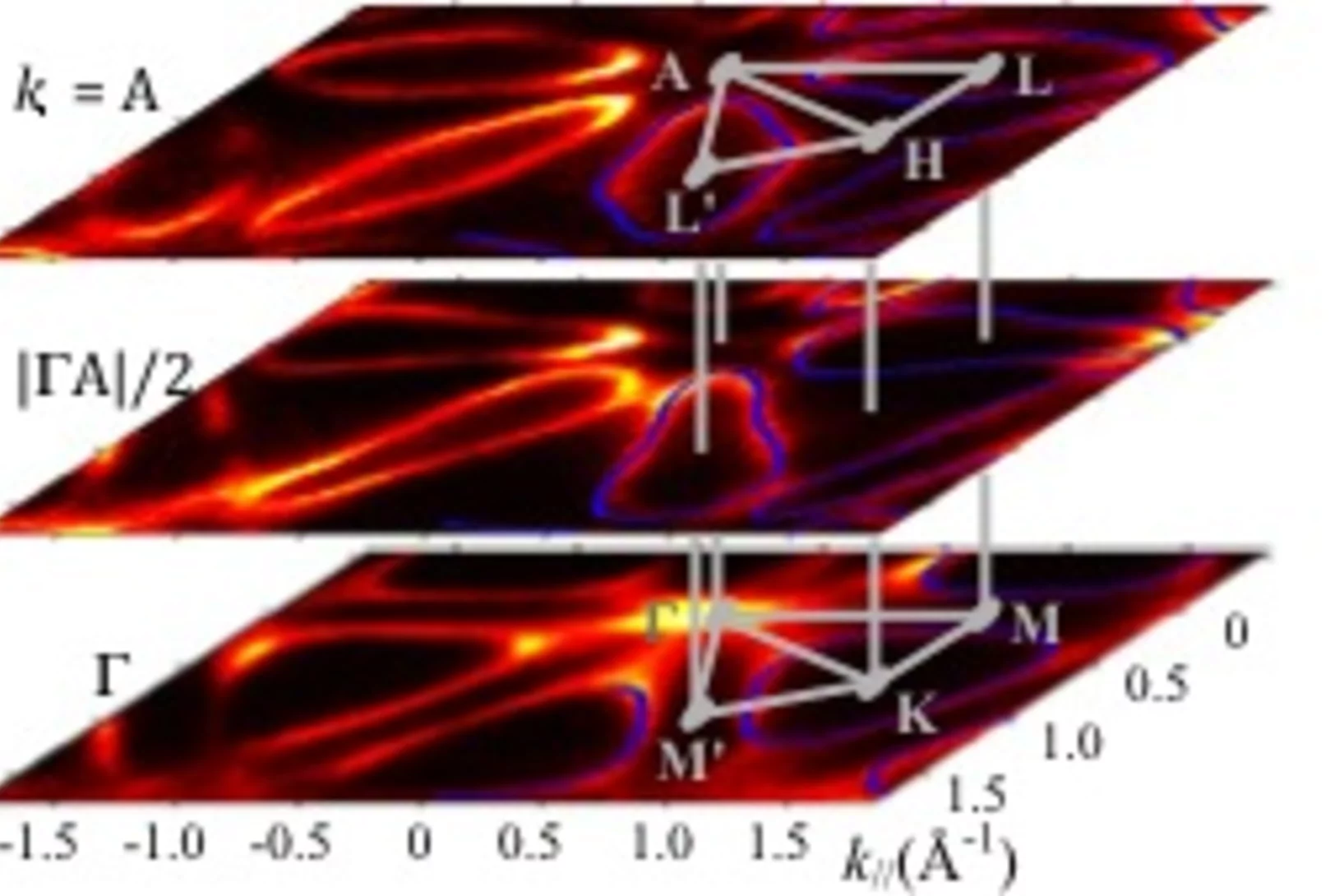
Three-Dimensional Electron Realm in Crystalline Solids Revealed with Soft-X-Rays
The electronic band structure E(k) as energy E of the electrons depending on its wavevector k is the cornerstone concept of the quantum solid state theory. The main experimental method to investigate E(k) is the angle-resolved photoelectron spectroscopy (ARPES). However, a small photoelectron escape depth of a few Å largely restricts the applications of ARPES to two-dimensonal crystals.
Laser-Induced Forward Transfer for the Fabrication of Devices
In conjunction with the increasing availability of cost-efficient laser units during the recent years, laser-based micromachining techniques have been developed as an indispensable industrial instrument of ‘‘tool-free’’ high-precision manufacturing techniques for the production of miniaturized devices made of nearly every type of materials. Laser cutting and drilling, as well as surface etching, have grown meanwhile to mature standard methods in laser micromachining applications where a well-defined laser beam is used to remove material by laser ablation. As an accurately triggerable nonmechanical tool, the ablating laser beam directly allows a subtractive direct-write engraving of precise microscopic structure patterns on surfaces, such as microchannels, grooves, and well arrays, as well as for security features. Therefore, laser direct-write (LDW) techniques imply originally a controlled material ablation to create a patterned surface with spatially resolved three-dimensional structures, and gained importance as an alternative to complementary photolithographic wet-etch processes. However, with more extended setups, LDW techniques can also be utilized to deposit laterally resolved micropatterns on surfaces, which allows, in a general sense, for the laser-assisted ‘‘printing’’ of materials.
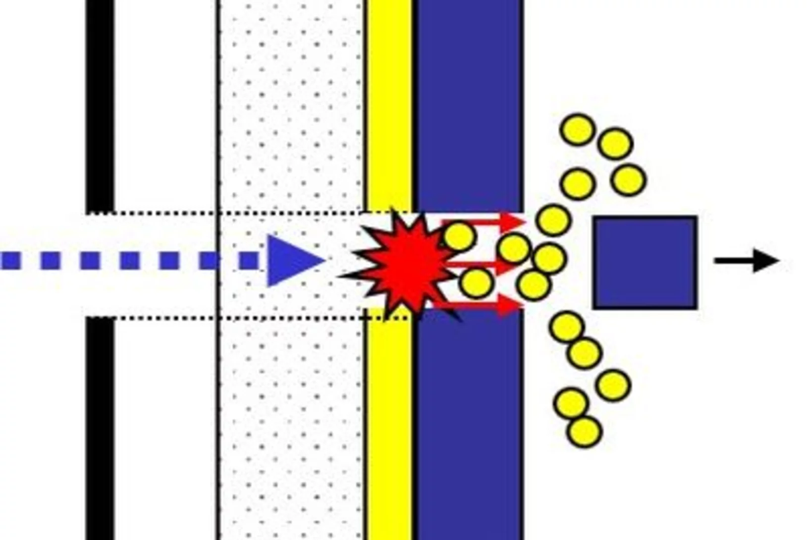
Supported gold as catalyst for the decomposition of ammonia precursors in the selective catalytic reduction of NOx
Titanium dioxide-supported gold was found to catalyze the hydrolysis of formate-based ammonia precursor compounds which are proposed for the selective catalytic reduction of nitrogen oxides (NOx) in combustion exhaust gas. In contrast to other noble metals, the supported gold does not oxidize the released NH3, while it maintains decomposition of intermediate formic acid.
Supported gold as catalyst for the decomposition of ammonia precursors in the selective catalytic reduction of NOx
Titaniumdioxide supported gold was found to catalyze the hydrolysis of formate-based ammonia precursor compounds which are proposed for the selective catalytic reduction of nitrogen oxides (NOx) in combustion exhaust gas. In contrast to other noble metals, the supported gold does not oxidize the released NH3, while it maintains decomposition of intermediate formic acid.

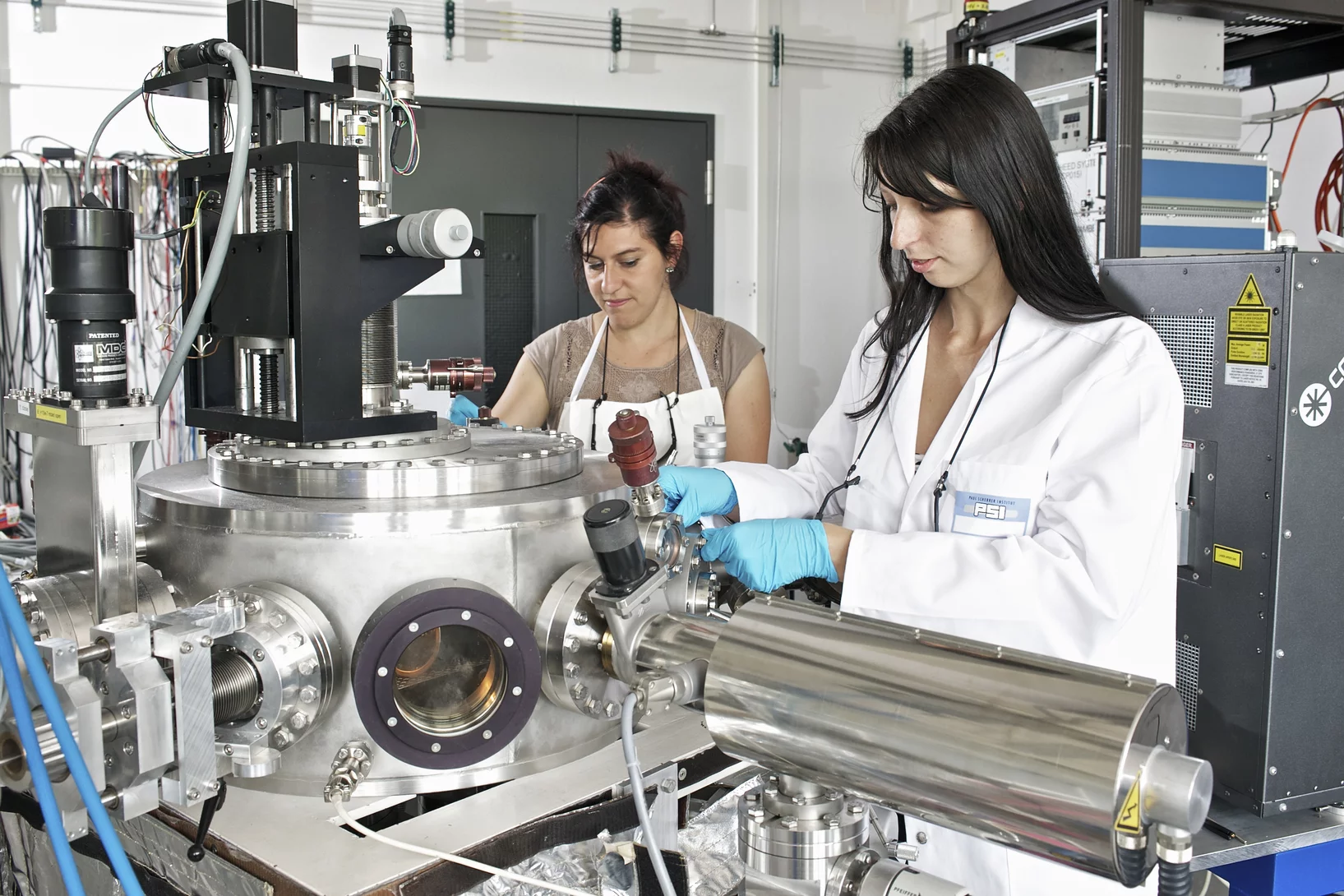
Ultra-short X-ray laser pulses precisely surveyed for the first time
X-ray lasers belong to a modern generation of light sources from which scientists in widely different disciplines expect to obtain new knowledge about the structure and function of materials at the atomic level. On the basis of this new knowledge, it could then be possible one day to develop better medicines, more powerful computers or more efficient catalysts for energy transformation.
Tunable conductivity threshold at polar oxide interfaces
The physical mechanisms responsible for the formation of a two-dimensional electron gas at the interface between insulating SrTiO3 and LaAlO3 have remained a contentious subject since its discovery in 2004. Opinion is divided between an intrinsic mechanism involving the build-up of an internal electric potential due to the polar discontinuity at the interface between SrTiO3 and LaAlO3, and extrinsic mechanisms attributed to structural imperfections.
Controversy clarified: Why two insulators together can transport electricity
How can two materials which do not conduct electricity create an electrically conducting layer when they are joined together? Since this effect was discovered in 2004, researchers have developed various hypotheses to answer this question – each with its own advocates, who defend it and try to prove its validity. Now, an international team under the leadership of researchers at the Paul Scherrer Institute has probably settled the controversy.
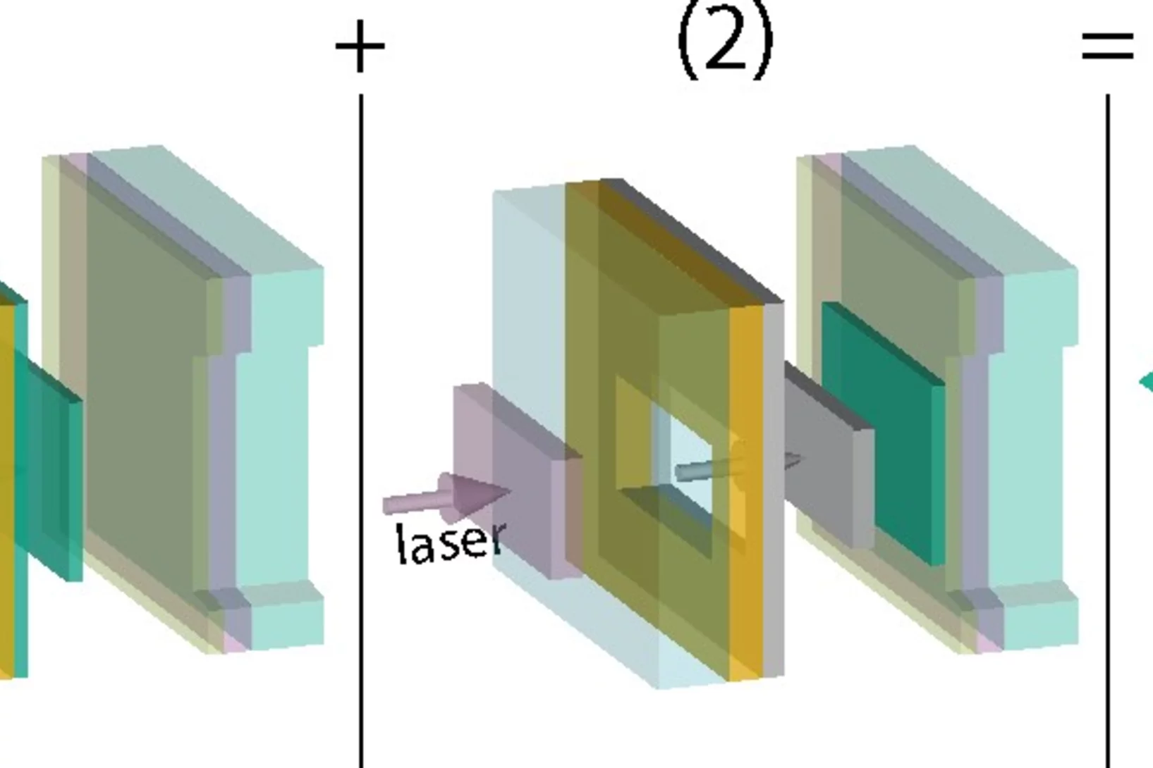
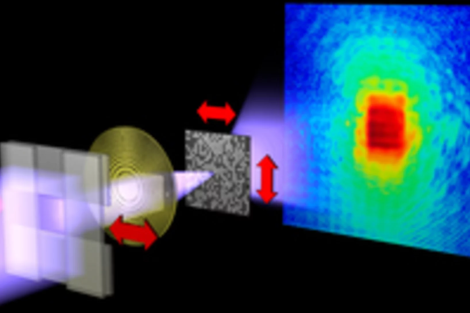
Sequential printing by laser-induced forward transfer to fabricate a polymer light-emitting diode pixel
Patterned deposition of polymer light-emitting diode (PLED) pixels is a challenge for electronic display applications. PLEDs have additional problems requiring solvent orthogonality of different materials in adjacent layers. We present the fabrication of a PLED pixel by the sequential deposition of two different layers with laser-induced forward transfer (LIFT), a “dry” deposition technique. This novel use of LIFT has been compared to “normal” LIFT, where all the layers are transferred in a single step, and a conventional PLED fabrication process.
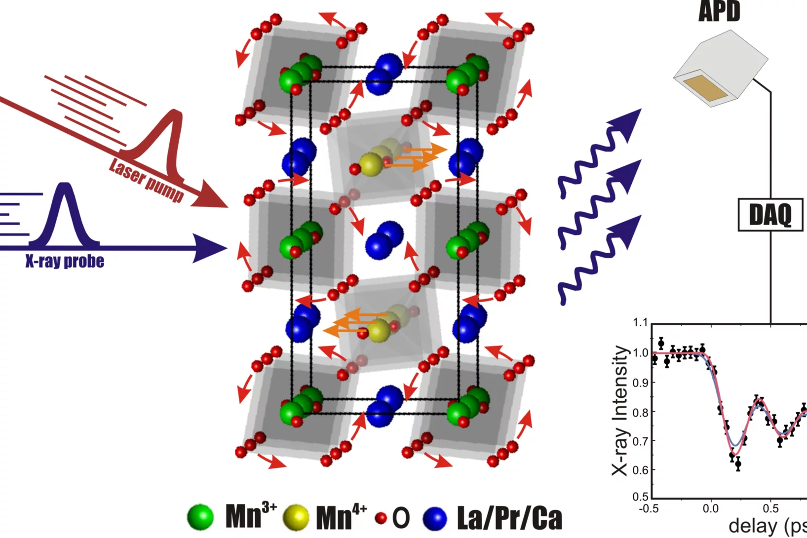
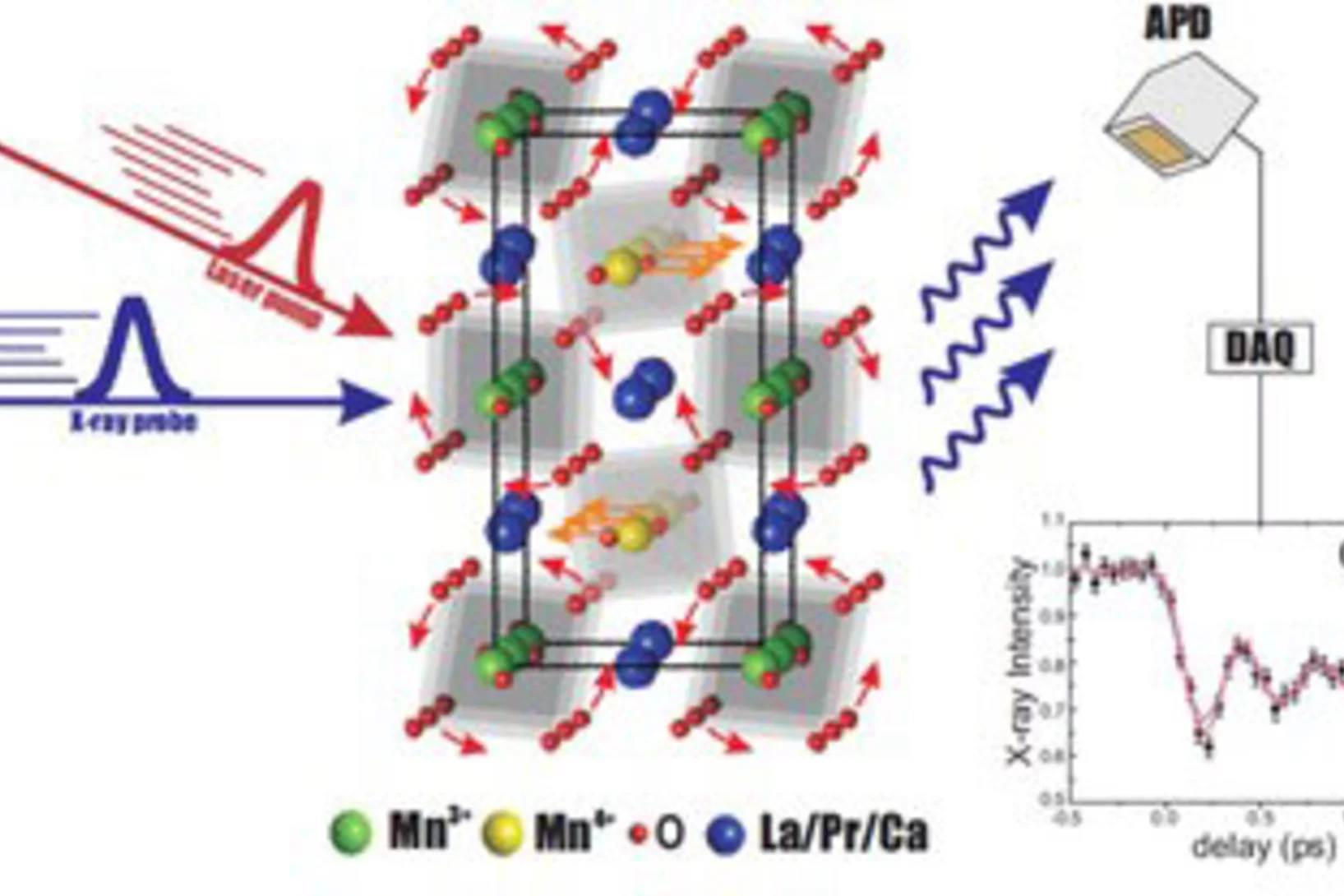
![(a) Mn K-edge XANES spectra of the ∼60 nm o-LMO epitaxial film were measured at room temperature for polarizations E || [110] and E || [001]. The inset shows the magnified pre-edge features. (b) FEFF simulations using the crystallographic data of the bulk o-LMO sample for E || [110] and E || [001]. The simulated pre-edges are shown on a larger scale in the inset.](/sites/default/files/styles/teaser_grid_3_2_crop_xl/public/import/lmx-interfaces/ScientificHighlights2012EN/YI_APL_2012.jpg.webp?itok=EjikdtFC)
Laser-Induced Forward Transfer for the Fabrication of Devices
X-ray near edge absorption spectroscopy was used to probe the electronic structure of multiferroic orthorhombic LuMnO3 polycrystalline samples and strained, twin-free orthorhombic (1–10) LuMnO3 films grown by pulsed laser deposition on (1–10) YAlO3 substrates. For all o-LuMnO3 samples x-ray near edge absorption spectroscopy spectra reveal that the pre-edge structure is influenced by the increase in MnO6 distortion as a result of the smaller Re-ion or film strain. Furthermore there is clear evidence of anisotropic Mn-O bonding and Mn orbital ordering along the c- and [110] direction. The experimental film and bulk data are in agreement with ab initio simulations.
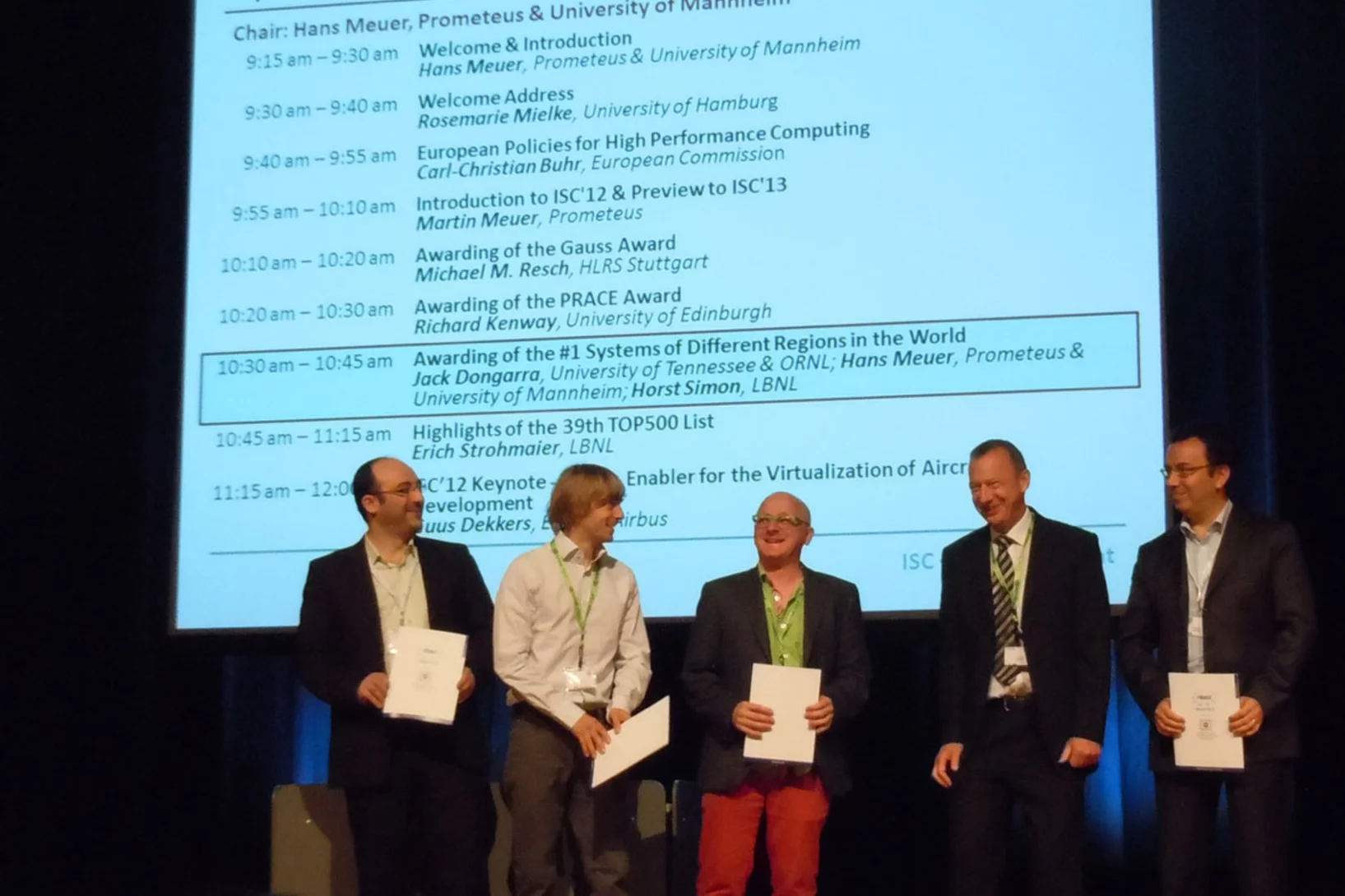
ETH Zurich, IBM and Paul Scherrer Institut Researchers receive 2012 PRACE Award
The MEGAWatt Pilot Experiment was operated for neutron generation with the PSI high intensity proton beam in 2006. The experiment utilized liquid target material, a lead bismuth eutectic. This marked a major milestone towards Accelerator Driven Systems (ADS), which are intended to be used for the incineration of nuclear waste.
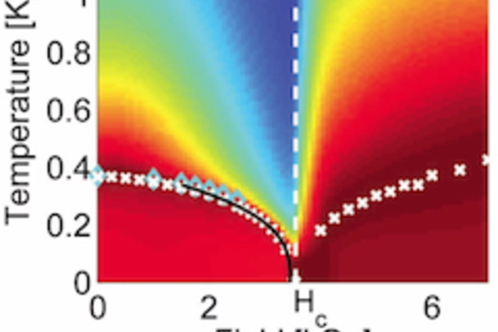
Dipolar Antiferromagnetism and Quantum Criticality in LiErF4
Magnetism has been predicted to occur in systems in which dipolar interactions dominate exchange. We present neutron scattering, specific heat, and magnetic susceptibility data for LiErF4, establishing it as a model dipolar-coupled antiferromagnet with planar spin-anisotropy and a quantum phase transition in applied field Hc|| = 4.0 ± 0.1 kilo-oersteds.
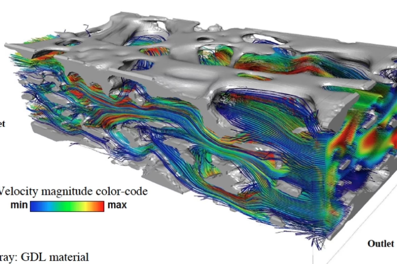
Flow modeling in gas diffusion layers of PEFCs at the micro- and mesoscale
he optimization of thermochemical and electrochemical conversion systems is of high importance for a sustainable energy future society. Of particular interest regarding the performance of polymer electrolyte fuel cells (PEFCs) is the study of the gas flow in the gas diffusion layers (GDL). More specifically, permeability and diffusivity measurements in a model PEFC under normal operating conditions are highly desirable. As laboratory-measurements of these quantities under such conditions are very demanding, an alternative is the use of computer-based simulations.
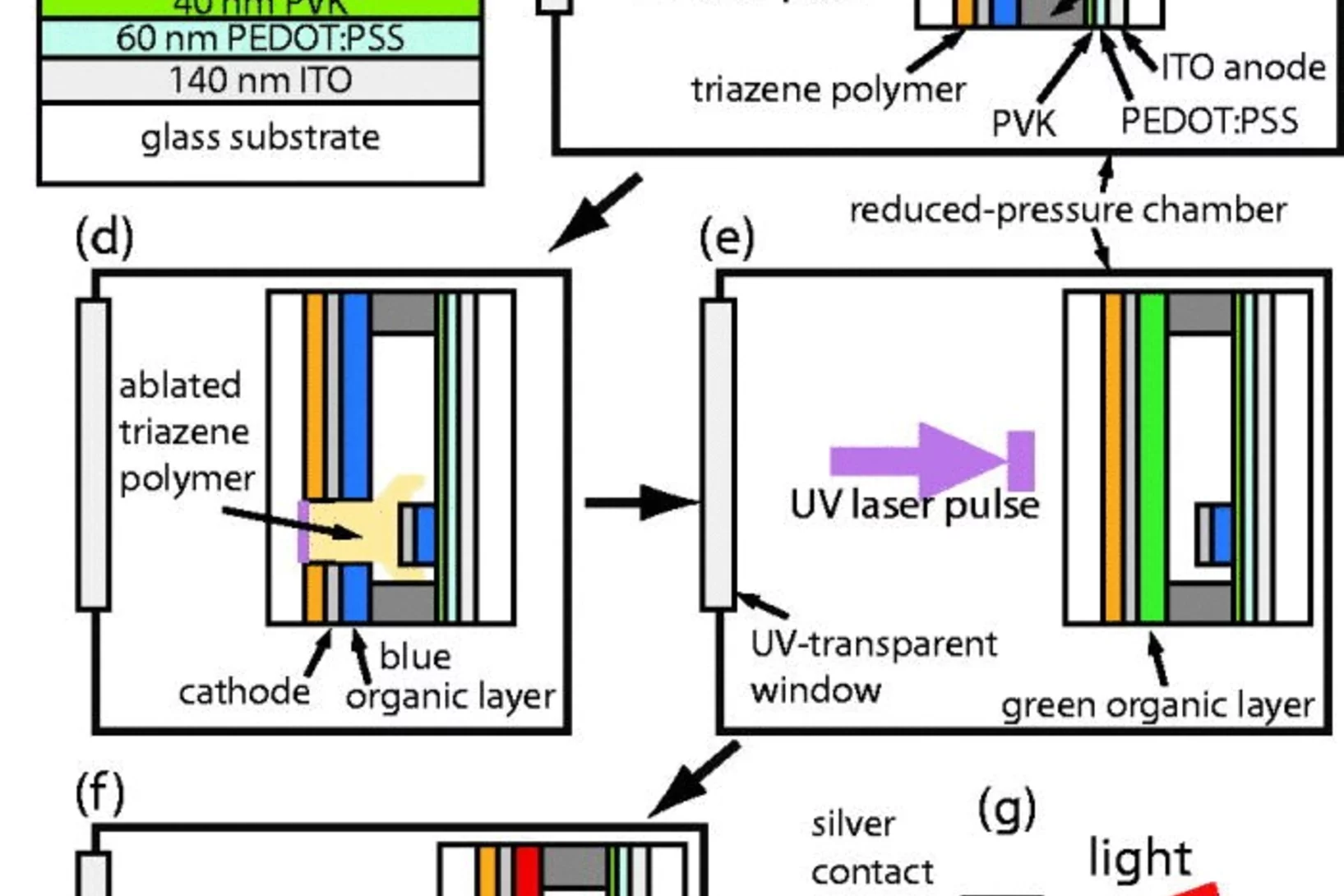
Red-green-blue polymer light-emitting diode pixels printed by optimized laser-induced forward transfer
An optimized laser-induced forward transfer (LIFT) technique has been used to fabricate tri-color organic light-emitting diode (OLED) pixels. At reduced pressures, and with a defined donor-receiver gap, patterned depositions of polyfluorene-based OLED pixels have been achieved. OLED pixel functionality has been demonstrated and compared with devices made using conventional deposition techniques. In addition, improved functionality has been obtained by coating the cathode with an electron-injecting layer, a process not possible using conventional OLED fabrication techniques. The OLED pixels fabricated by LIFT reach efficiencies on the range of conventionally fabricated devices and even surpass them in the case of blue pixels.
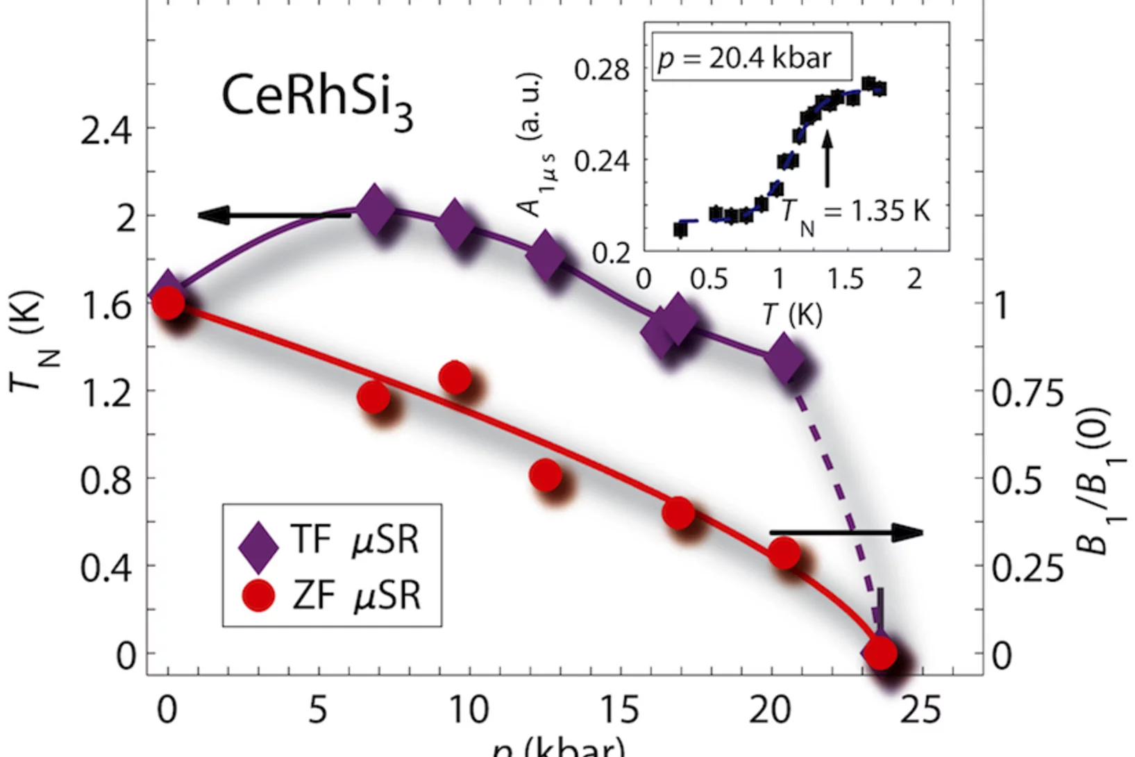
Direct observation of the quantum critical point in heavy fermion CeRhSi3
In many heavy fermion materials the quantum critical point is masked by superconductivity and it can only be detected by use of a local probe. In the noncentrosymmetric heavy fermion CeRhSi3 the ground state at ambient pressure is antiferromagnetically ordered and superconductivity sets in above 12 kbar coexisting with antiferromagnetism. We have unraveled a magnetic quantum critical point hidden deep inside the superconducting state of CeRhSi3.
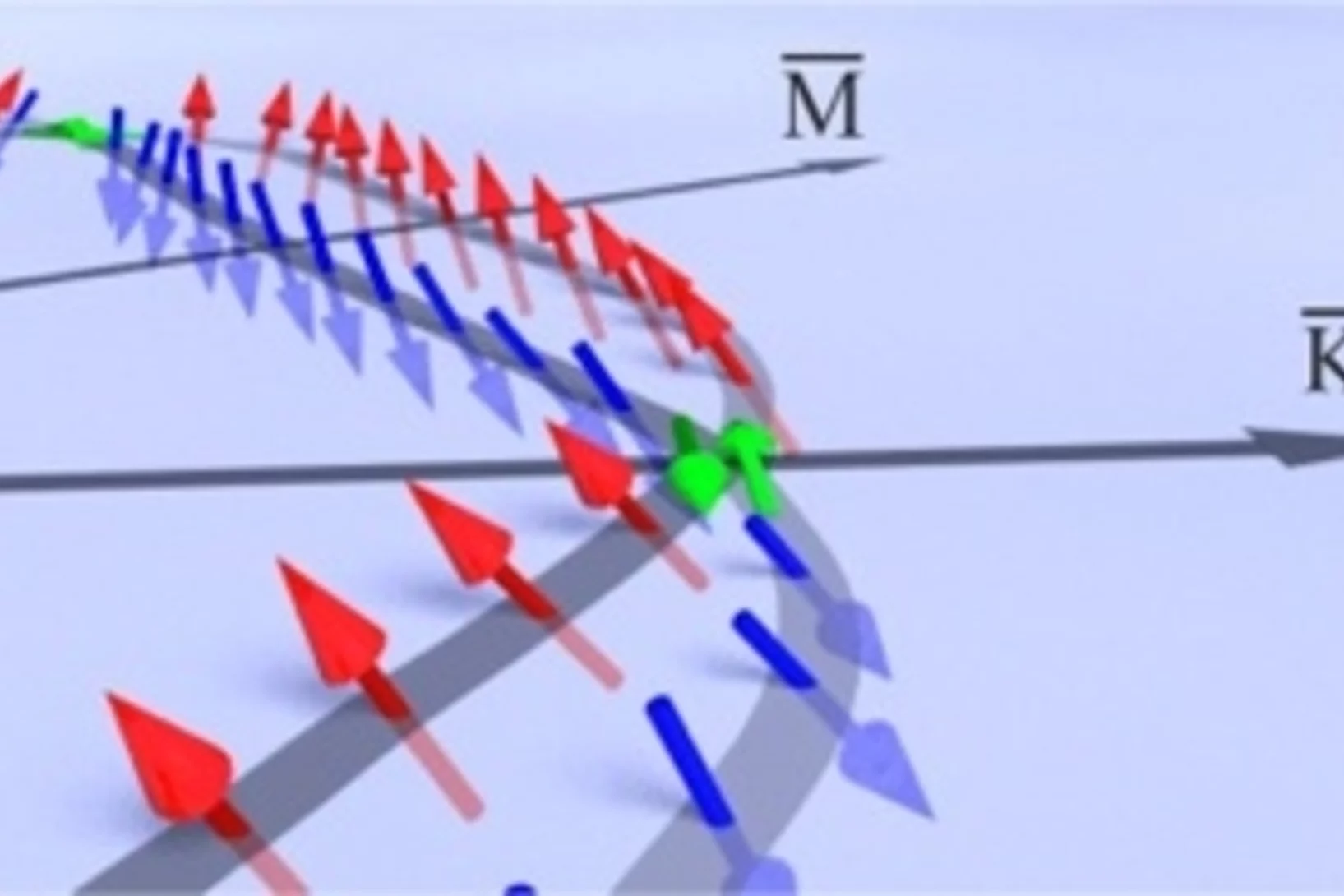
Three-Dimensional Spin Rotations in a Monolayer Electron System
In the emerging field of spintronics, the generation, injection, and in particular the control of highly spin polarized currents are main issues to be solved. Lifting of spin degeneracy by the spin-orbit interaction at surfaces, known as Rashba effect, represents a promising approach, since it generates two spin-polarized bands without the necessity of an external field. In our recent study, we realize such a system for a metallic surface layer on a semiconductor: Au/Ge(111).
Physicists observe the splitting of an electron inside a solid
An electron has been observed to decay into two separate parts, each carrying a particular property of the electron: a spinon carrying its spin – the property making the electron behave as a tiny compass needle – and an orbiton carrying its orbital moment – which arises from the electron’s motion around the nucleus. These newly created particles, however, cannot leave the material in which they have been produced.
Ellipsoidal hybrid magnetic microgel particles with thermally tunable aspect ratios
We report on the synthesis and characterization of multiresponsive hybrid microgel particles. The particles consist of ellipsoidal silica-coated maghemite cores subsequently coated with thermoresponsive poly (N-isopropylacrylamide) (PNIPAM) shells. The PNIPAM shell enables the hybrid particle to alter its size and ratio of long to small axis with increasing temperature while the core morphology remains unchanged.
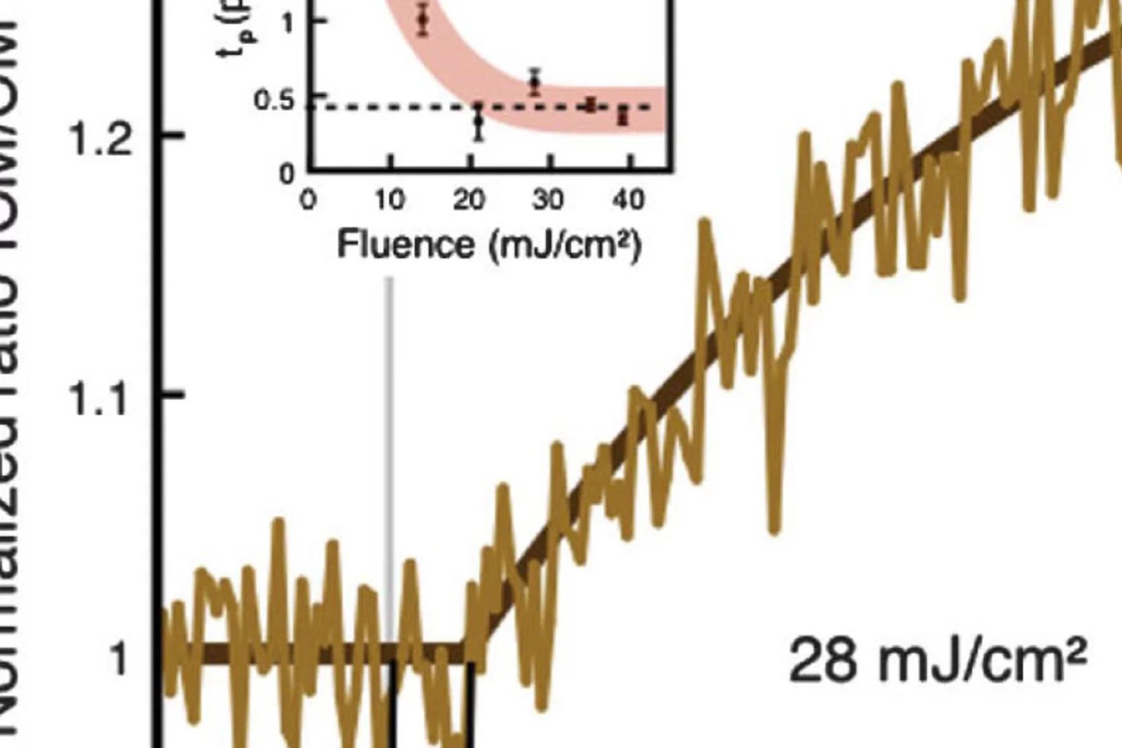
Structural and magnetic dynamics of a first order phase transition
We use time-resolved x-ray diffraction and magneto-optical Kerr effect to study the laser-induced antiferromagnetic to ferromagnetic phase transition in FeRh. The structural response is given by the nucleation of independent ferromagnetic domains (t ~ 30 ps).
Creating magnetism takes much longer than destroying it
Researchers at the Paul Scherrer Institute are finding out how long it takes to establish magnetism and how this happens.

Directly coupled Ferromagnetism and Ferroelectricity in the Olivine Mn2GeO4
The olivine compound Mn2GeO4 is shown to feature both a ferroelectric polarization and a ferromagnetic magnetization that are directly coupled and point along the same direction. We show that a spin spiral generates ferroelectricity, and a canted commensurate order leads to weak ferromagnetism.

Origin of the Large Polarization in Multiferroic YMnO3 Thin Films
Multiferroic materials have attracted much interest because of their ability to control magnetism by the application of an electric field. This ability is expected to reduce the power required by electronic devices and to increase their speed. However, the number of multiferroic materials discovered so far has been small, and ferromagnetism and ferroelectricity in the known materials are often much weaker than required for practical applications.
Liquids in narrow spaces
How does spatial confinement affect the microscopic structure of liquids?
This is a question which is receiving increasing attention from condensed matter physicists. Liquids are characterized by a short-ranged, so-called local structure, and it has been predicted theoretically about 25 years ago that confinement induces anisotropy in the local structure, and hence many properties, of liquids.
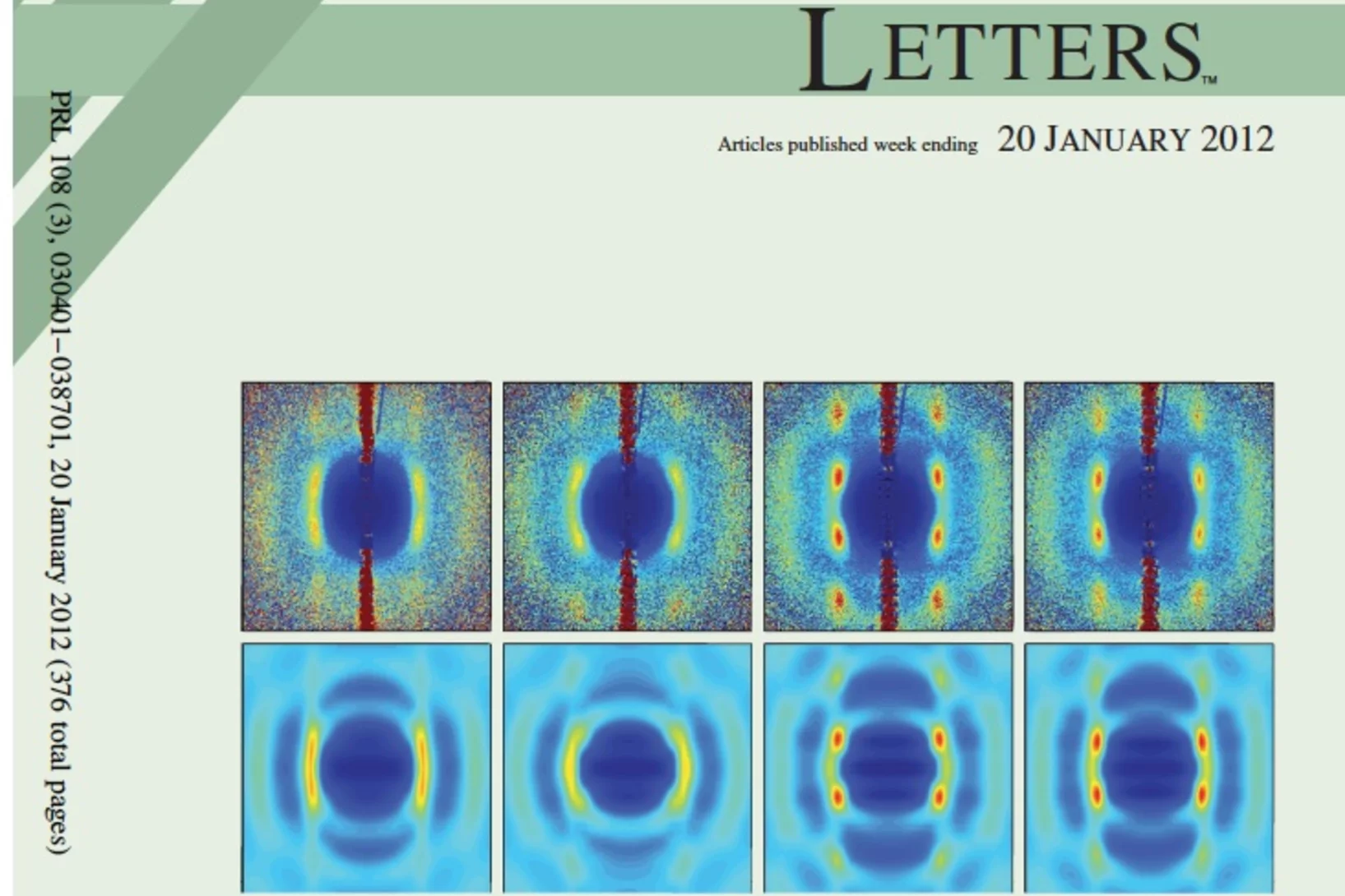
Femtosecond dynamics of an antiferromagnetic phase transition
We report on the ultrafast dynamics of magnetic order in a single crystal of CuO at a temperature of 207 K in response to strong optical excitation using femtosecond resonant x-ray diffraction. In this experiment performed at the LCLS X-ray free electron laser at Stanford a femtosecond laser pulse induces a sudden, nonequilibrium increase in magnetic disorder.

A close look at correlated electrons in heavy-fermion metal through ARPES
Showing astonishing properties like magnetism, superconductivity, Kondo and heavy-fermion (HF) behavior, rare-earth intermetallic compounds have been at the forefront of modern solid state physics for many years. Most of these properties are related to a delicate interplay between the partially filled 4f-shell and conduction electrons.
Vertical Emittance of the SLS Storage Ring
On the 6th of December 2011 the vertical emittance of the SLS storage ring could be reduced to a world record low value of 1pm rad. The vertical beam size in the short straight sections of the SLS is then only 3 micron (rms). This was achieved through vertical re-alignment of the magnet girders with 400mA stored beam and fast orbit feedback running, as well as through application of several different methods of coupling suppression using 36 skew quadrupoles. High resolution profile monitor utilizing vertically polarized component of synchrotron radiation allowed precise determination of the beam size.
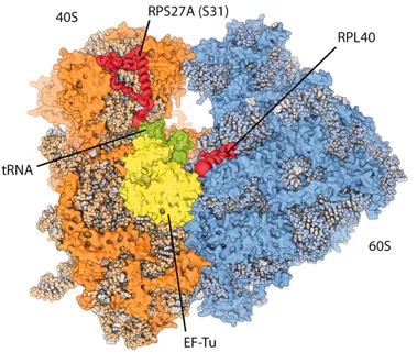
New insights into the cell’s protein factory
Eukaryotic ribosomes are among the most complex cellular machineries of the cell. These large macromolecular assemblies are responsible for the production of all proteins and are thus of pivotal importance to all forms of life. Two independent research groups at the ETH Zürich and the Institute of Genetics and Molecular and Cellular Biology in Strasbourg have obtained new insights into the atomic structure of the eukaryotic ribosome. The results have been published in the journal Science.