

The group’s research activity combines different spectroscopies and microscopie to investigate surfaces and interfaces down to the atomic scale:
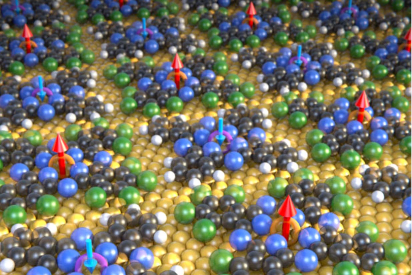
- Controlling electron and spin‐based quantum states in surface supported molecular and supramolecular architectures by chemical and/or physical switches. Specific, low-dimensional, atomic and supramolecular architectures at surfaces and interfaces are characterized in order to under‐ stand the mechanisms ruling their response and cooperative action in conjunction with topo‐ logical, surface and interface states. Density Functional Theory (DFT)+U calculations per‐ formed by our collaborators give a very important input to achieve this goal.
- Investigate fundamental processes in applied processes and devices down to the atomic scale. Atomic‐level structure, diffusion and processes decisively affect the performance of functional materials and devices. Examples have been provided by resist materials, high‐power semiconductor, organic electronic and medical devices. Spectro‐microscopy correlation here can provide new fundamental insight and contribute to novel and/or improved function or functionality.
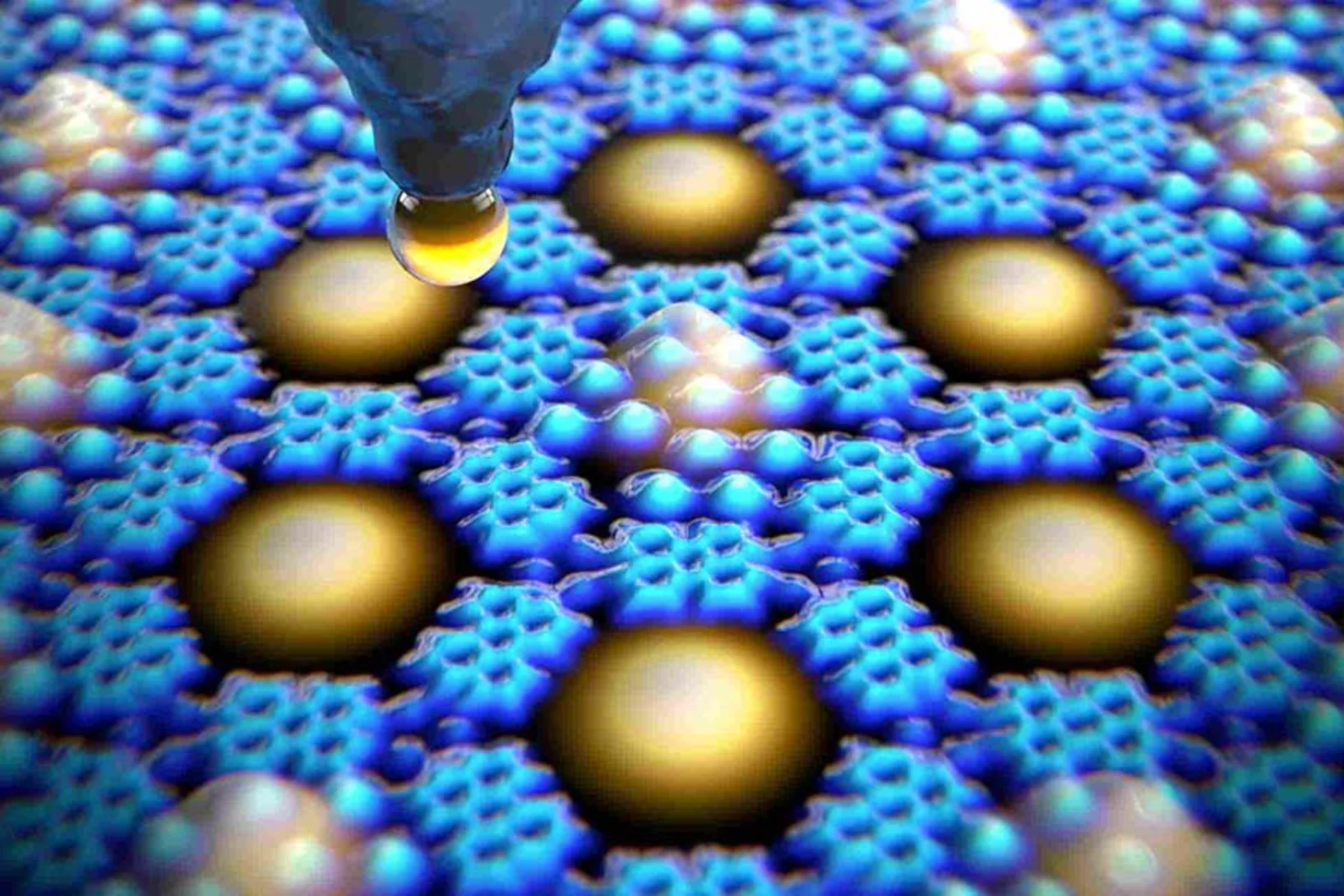
- Supramolecular architecturing of novel materials and in particular quantum materials. In close collaboration with chemists, chemically programmed supramolecular assembly has al‐ lowed us to create unprecedented low dimensional materials with unique properties i.e. 2D spin array and ferrimagnets and free standing layers with programmable architecture and chemical functions, also for the inspection of single molecules and nanoparticles (so called sample delivery).
The group has built the competence and infrastructure to make and investigate materials architectured from a wide range of components i.e. elements, compounds and programmed organic molecules. The assembly and operation of nanomaterials and nanodevices is investigated by a broad range of mechani‐ cal, magnetic, and electronic properties are studied using surface sensitive techniques: X‐ray Photoelectron Spectroscopy (XPS), Scanning Probe Microscopy (SPM), X‐ray Magnetic Circular Dichroism (XMCD) spectroscopy, Angle Resolved Photoemission Spectroscopy (ARPES), Low‐Energy and others. As of 01.07.2017, the group operates the PEARL beamline of the Swiss Light Source.
News and Highlights


Video clips about our science
- New Class of Materials for Redox Reactions
- Data Storage with molecules: Phase Transitions in Confinements
- Local Manipulation of Spin Domains in a Multiferroic Rashba Semiconductor
- Emergence of On-Surface Magnetochemistry
Video clips by the swiss nanoscience institute containing material from our group
Research Areas
Facilities
- Surface Science Lab at Laboratory for Micro-and Nanotechnology
- Scanning Probe Microscopy Userlab at Laboratory for Micro-and Nanotechnology
- PEARL* beamline of the Swiss Light Source.
Related facility instrumentation
Collaborations
- Prof. Dr. G. Morgan CSCB_UCD Dublin
- Prof. Dr. N. Ballav IISER Pune
- Prof. Dr. P. Oppeneer Uppsala University
- Prof. Dr. F. Nolting Swiss Light Source
- Prof. Dr. F. Diederich ETH Zurich
- Prof. Dr. L. H. Gade Heidelberg University
- Prof. Dr. E. Meyer University of Basel
- Prof. Dr. S. Goedecker University of Basel
- Prof. Dr.-Ing. J. Gobrecht PSI LMN and INKA
- Prof. S. Decurtins, Dr. Shi-Xia LIU University of Bern
- Dr. A. Kleibert Swiss Light Source
- Dr. J. Dreiser Swiss Light Source
- Dr. C. Piamonteze Swiss Light Source
- Dr. J. Raabe Swiss Light Source
- Dr. Hans Sigg, Dr. M. Camarda, J. Wörle PSI LMN
- Dr. H. Bartolf, Dr. J. Lehmann, Dr. R. A. Minamisawa ABB Switzerland
- Dr. A. Schöner Ascatron Switzerland
- Dr. S. Gerstl EMEZ ETH Zurich
Selected Publications
Evidence for carbon clusters present near thermal gate oxides affecting the electronic band structure in SiC-MOSFET
Dutta D, De D, Fan D, Roy S, et al.
Appl. Phys. Lett. 115, 101601 (2019)
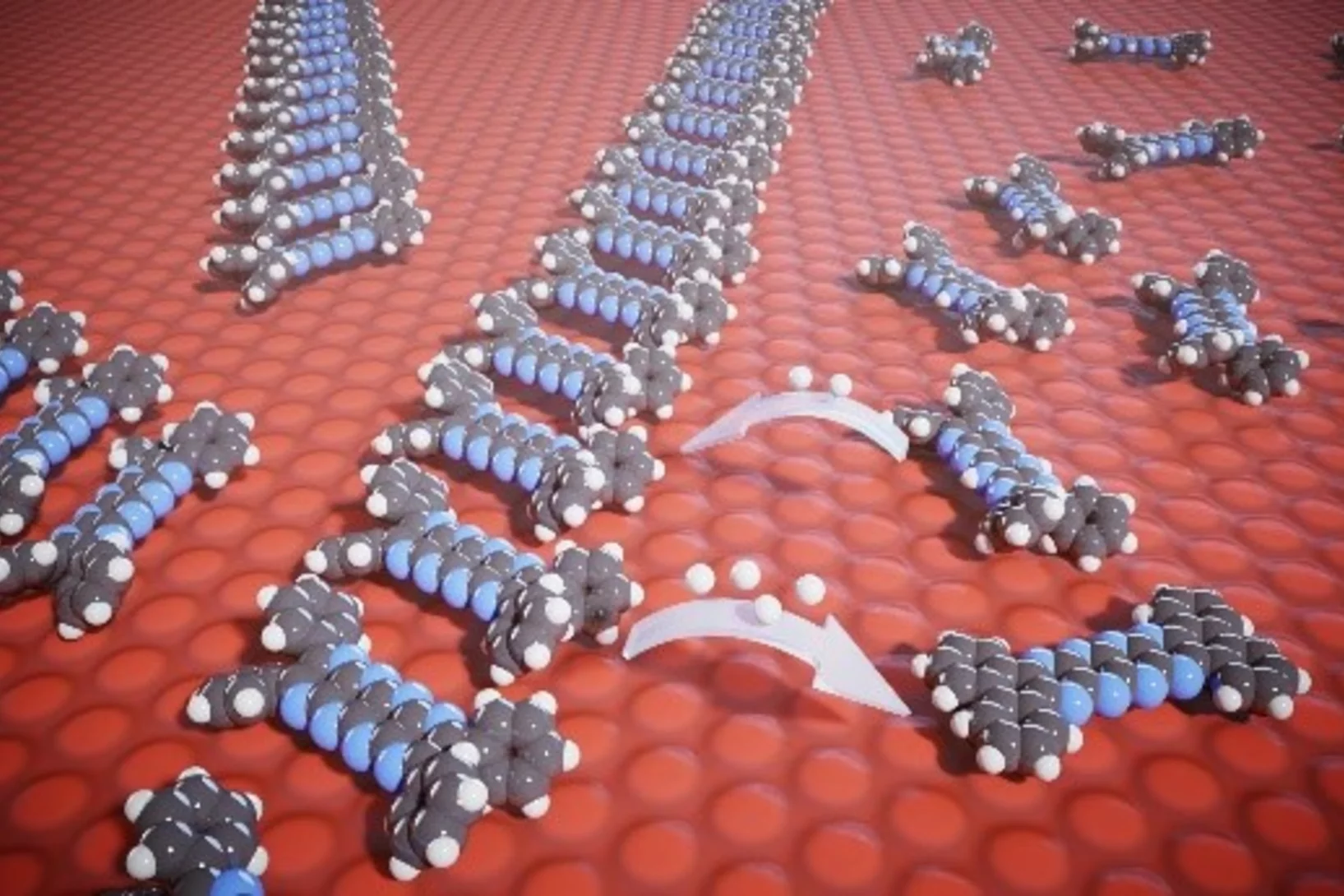
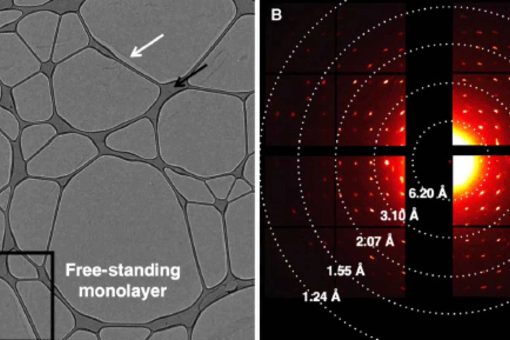
Supramolecular architectures of molecularly thin yet robust free-standing layers
Moradi M, Opara N, Tulli L, Wäckerlin C, et al.
Sci. Adv. 5: eaav4489 (2019)
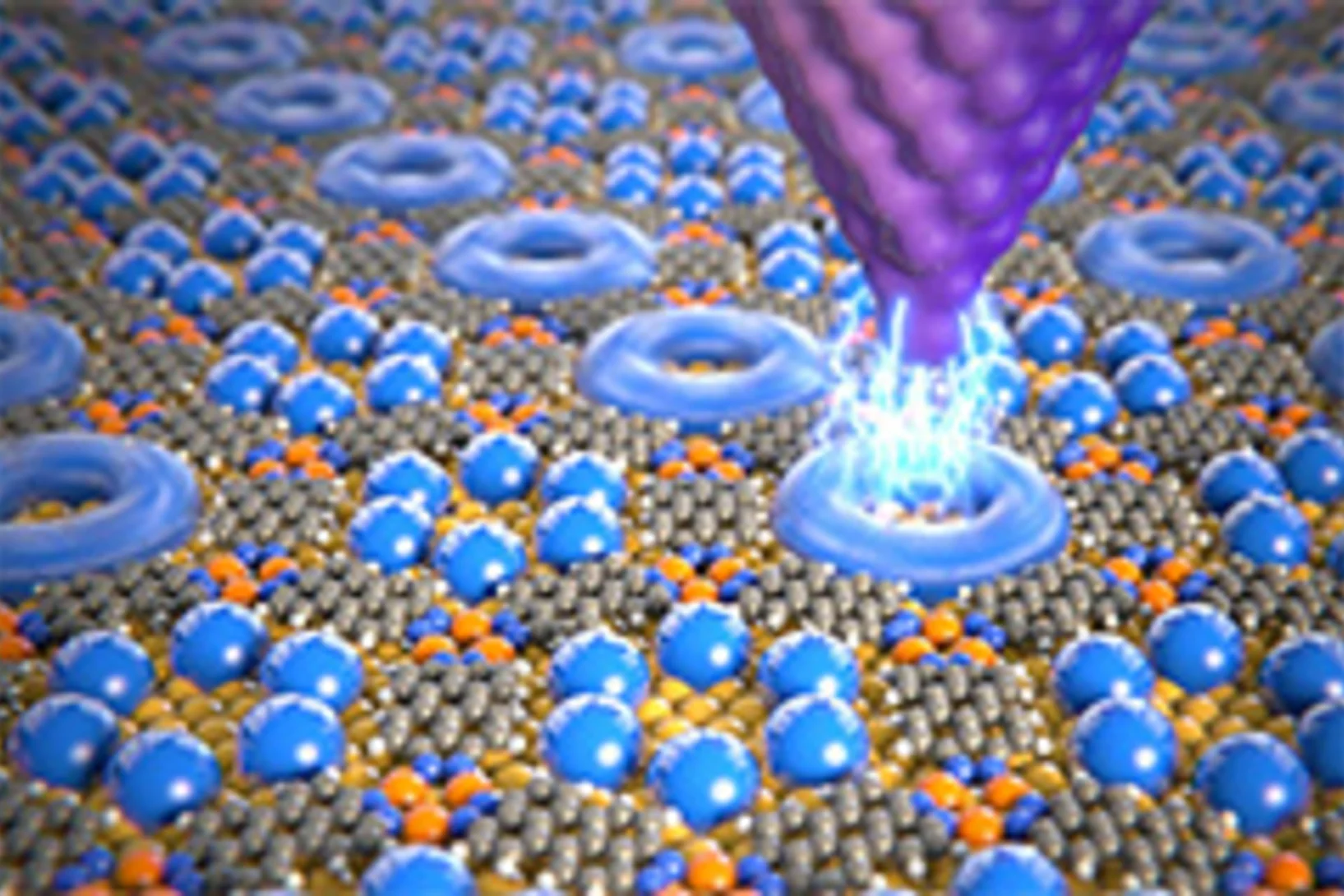
Adsorbate-Induced Modification of the Confining Barriers in a Quantum Box Array
Nowakowska S, Mazzola F, Alberti M, Song F, et al.
ACS Nano. 12 (1), 768 (2018)
On the needle clogging of staked-in-needle pre-filled syringes: Mechanism of liquid entering the needle and solidification process
Bardi M, Müllera R, Grünzweigc C, Mannesc D, et al
EUR J PHARM BIOPHARM. 128,272 (2018)
Long-range ferrimagnetic order in a two-dimensional supramolecular Kondo lattice
Girovsky J, Nowakowski J, Ali MdEhesan, Baljozovic M, et al.
Nat. Commun. 8, 15388 (2017)
Surface science at the PEARL beamline of the Swiss Light Source
Muntwiler M, Zhang J, Stania R, Matsui F, et al.
J. Synchrotron Rad. 24, 354 (2017)
Device Simulations on Novel High Channel Mobility 4H-SiC Trench MOSFETs and Their Fabrication Processes
H. R. Rossmann, A. Bubendorf, F. Zanella, N. Marjanović, et al.
Microelectron. Eng. 145, 166 (2015)
Interplay of weak interactions in the atom-by-atom condensation of xenon within quantum boxes
S. Nowakowska, A. Waeckerlin, S. Kawai, T. Ivas, J. Nowakowski, et al.
Nat. Commun. 6, 6071 (2015)
Antiferromagnetic coupling of Cr-porphyrin to a bare Co substrate
J. Girovsky, K. Tarafder, C. Waeckerlin, J. Nowakowski, D. Siewert et al.
Phys. Rev. B 90, 220404 (2014)
On-surface synthesis of a two-dimensional porous coordination network: Unraveling adsorbate interactions
M. Matena, J. Bjork, M. Wahl, T-L. Lee, J. Zegenhagen, L. H. Gade, et al.
Phys. Rev. B 90, 125408 (2014)
Exchange Interaction of Strongly Anisotropic Tripodal Erbium Single-Ion Magnets with Metallic Surfaces
J. Dreiser, C. Waeckerlin, Md. E. Ali, C. Piamonteze, F. Donati, et al.
ACS Nano 8, 4662 (2014)
Covalent assembly of a two-dimensional molecular "sponge" on a Cu(111) surface: confined electronic surface states in open and closed pores
A. Shchyrba, S. C. Martens, C. Waeckerlin, M. Matena, T. Ivas, et al.
Chem. Commun. 50, 7628 (2014)
Controlling the Dimensionality of On-Surface Coordination Polymers via Endo- or Exoligation
A. Shchyrba, C. Waeckerlin, J. Nowakowski, S. Nowakowska, et al.
J. Am. Chem. Soc. 136, 9355 (2014)
Investigating magneto-chemical interactions at molecule-substrate interfaces by X-ray photo-emission electron microscopy
J. Girovsky, M. Buzzi, C. Waeckerlin, D. Siewert, J. Nowakowski, et al.
Chem. Commun. 50, 5190 (2014)
Two-Dimensional Supramolecular Electron Spin Arrays
C. Waeckerlin, J. Nowakowski, S-X. Liu, J. Michael, D. Siewert, et al.
Adv. Mater. 25, 2404(2013)
Porphyrin metalation providing an example of a redox reaction facilitated by a surface reconstruction
J. Nowakowski, C. Wäckerlin, J. Girovsky, D. Siewert, T. A. Jung, N. Ballav
Chem. Commun. 49, 2347 (2013)
Emergence of On-Surface Magnetochemistry
N. Ballav, C. Wäckerlin, D. Siewert, P. M. Oppeneer, T. A. Jung
J. Phys. Chem. Lett. 4, 2303 (2013)