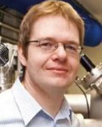
Biography
Jörg Raabe is heading the Microspectroscopy Group of the Laboratory for Condensed Matter in the Photon Science Division since 2008. He received his PhD from the University of Regensburg in 2003 working on low dimensional electron systems and magnetic nano structures. Afterwards he initially worked as Postdoc at the SIM beamline of the SLS, before he started the construction of the PolLux beamline as beamline scientist in 2005.
Institutional Responsibilities
The main responsibility is the managing and running the in-house and user program at the PolLux and the the In Situ Spectroscopy beamlines of the SLS. Besides this, Jörg Raabe is strongly involved in the development of advanced x-ray microscopy instruments.
Scientific Research
Jörg Raabe's scientific research is focused on x-ray microscopy of magnetic systems with a special focus on time resolved studies. The topics cover e.g. spin waves and skyrmions.
Selected Publications
For an extensive overview we kindly refer you to our publication repository DORA.
From 2D STXM to 3D imaging: soft X-ray laminography of thin specimens, Witte, K., Späth, A., Finizio, S., Donnelly, C., Watts, B., Sarafimov, B., … Raabe, J. Nano Letters, 20(2), 1305-1314 (2020). https://doi.org/10.1021/acs.nanolett.9b04782
Soft X-ray 3D imaging has already been realized at synchrotron radiation sources using either scanning transmission X-ray microscopy (STXM) schemes or tomography-based concepts. However, the maximum accessible sample volume is severely limited by the reduced penetration depth of the lower-energy soft X-ray radiation. This becomes even more of a drawback in the case of flat and extended specimens, which can be found in various fields of nanoscience.
The generalized geometry of laminography, characterized by a tilted axis of rotation concerning the incident X-ray beam resulting in a constant material thickness during rotation, has proven to be particularly suitable for the investigation of laterally extended and thin objects. The combination of soft X-rays and laminography provides the unique potential of bridging the gap between investigations of elaborate nanostructured thin film samples and taking advantage of the characteristic absorption contrast mechanisms in the soft X-ray range.
Deterministic Field-Free Skyrmion Nucleation at a Nanoengineered Injector Device
Simone Finizio, Katharina Zeissler, Sebastian Wintz, Sina Mayr, Teresa Weßels, Alexandra J. Huxtable, Gavin Burnell, Christopher H. Marrows, Jörg Raabe. Nano Letters (2019). https://doi.org/10.1021/acs.nanolett.9b02840
Magnetic skyrmions are topologically non-trivial quasi-particles with a set of properties that makes them promising for applications as encoders for digital information. As a result of this, many different skyrmion-based memory and computation designs have recently been proposed. All of these applications, however, depend on a reproducible and reliable nucleation, displacement, detection, and deletion of the topological quasi-particles. While the displacement and detection of magnetic skyrmions have been thoroughly investigated, also at the PolLux endstation, no major attention has been given to the investigation and optimization of the skyrmion nucleation process.
High-resolution non-destructive three-dimensional imaging of integrated circuits, Mirko Holler, Manuel Guizar-Sicairos, Esther H. R. Tsai, Roberto Dinapoli, Elisabeth Müller, Oliver Bunk, Jörg Raabe & Gabriel Aeppli, Nature 543, 402–406, (2017), doi:10.1038/nature21698
Modern nanoelectronics has advanced to a point at which it is impossible to image entire devices and their interconnections non-destructively because of their small feature sizes and the complex three-dimensional structures resulting from their integration on a chip. Here we demonstrate that X-ray ptychography—a high-resolution coherent diffractive imaging technique—can create three-dimensional images of integrated circuits of known and unknown designs with a lateral resolution in all directions down to 14.6 nanometres. Our experiments represent a major advance in chip inspection and reverse engineering over the traditional destructive electron microscopy and ion milling techniques.


