

Electronic properties of van der Waals (vdW) materials can be influenced by external parameters such as the stacking order, gating and the twist angle between the sheets. The latter introduces a new moiré superlattice structure in real space along with flat energy bands and a high density of states in reciprocal space which can give rise to collective behavior and exotic ground states. Hence, vdW devices are an ideal platform to engineer quantum many-body states to study strongly correlated physics and topology.

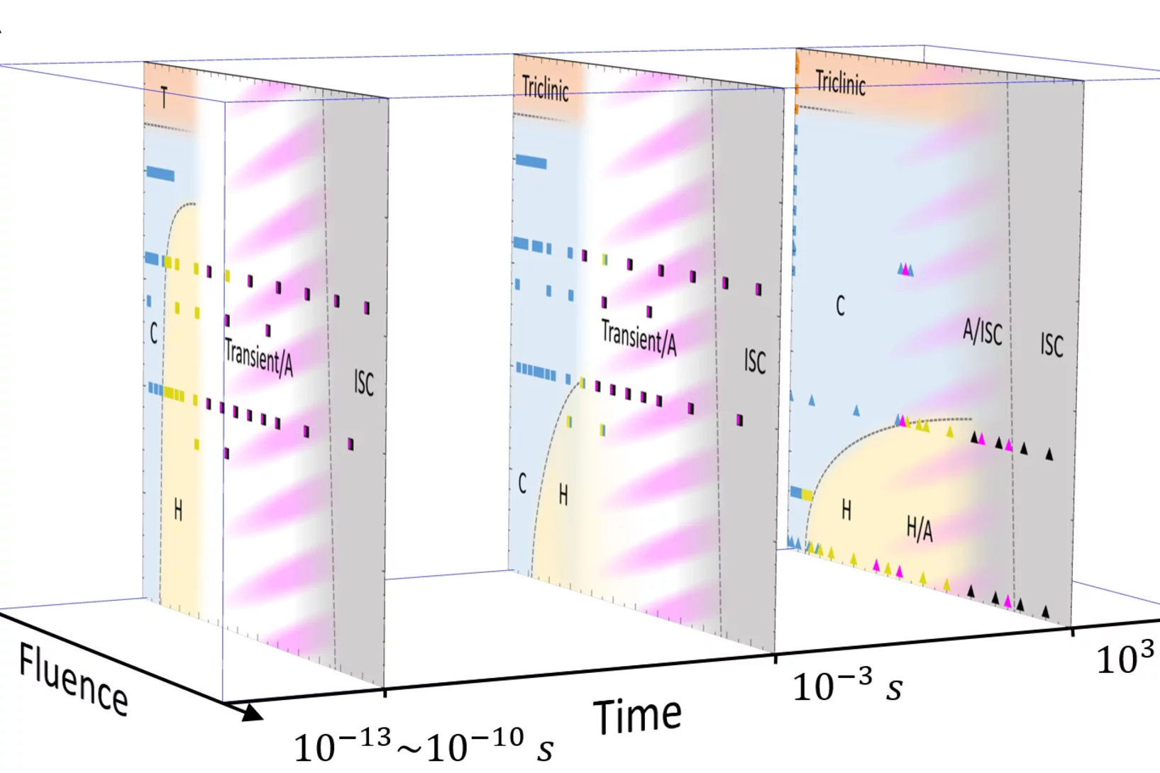
1T-TaS2 is a layered transition metal dichalcogenide, which exhibits a variety of equilibrium states, ranging from metallic at high temperature, a series of charge-density wave (CDW) states at intermediate temperatures and an insulating Mott state below 180 Kelvin. Intriguingly, a variety of long-lived metastable photo- and electrically-induced states are found, which are stable at low temperatures.
In this project, we investigate the photo- and electrically-induced so-called “hidden” state of 1T-TaS2, which has orders of magnitude lower resistivity than the thermodynamically stable insulating low-temperature state. The transition to this photoinduced state occurs on sub-picosecond timescale, making the material an ideal candidate for ultrafast low-energy non-volatile cryomemory devices. We work in collaboration with the Jozef Stefan Institute where the material is synthesized and characterized using optical methods and scanning tunneling microscopy. For device fabrication, we use PSI’s PICO cleanroom facilities and employ synchrotron and X-ray free-electron laser techniques to shine light on the equilibrium and non-equilibrium physics.
Recent publications & preprints
Interlayer stacking controls the electronic properties of the van der Waals material 1T-TaS2
N. Hua, F. Petocchi, H. G. Bell, G. Aeppli, P. Werner, S. Gerber
Phys. Rev. Research 8, L012047 (2026)
Imaging of electrically controlled van der Waals layer stacking in 1T-TaS2
C. Burri, N. Hua, D. Ferreira Sanchez, W. Hu, H. G. Bell, R. Venturini, S.-W. Huang, A. G. McConnell, F. Dizdarevic, A. Mraz, D. Svetin, B. Lipovsek, M. Topic, D. Kazazis, G. Aeppli, D. Grolimund, Y. Ekinci, D. Mihailovic, S. Gerber
Nat. Commun. 16, 10296 (2025)
Three-dimensional electronic domain correlations in 1T-TaS2
C. Burri, H. G. Bell, F. Dizdarević, W. Hu, J. Ravnik, J. Vonka, Y. Ekinci, S.-W. Huang, S. Gerber, N. Hua
arXiv:2508.17839
Van der Waals devices for surface-sensitive experiments
N. Taufertshöfer, C. Burri, R. Venturini, I. Giannopoulos, S. A. Ekahana, E. Della Valle, A. Mraz, Y. Vaskivskyi, J. Lipic, A. Barinov, D. Kazazis, Y. Ekinci, D. Mihailovic, S. Gerber
Nanoscale 17, 19957 (2025)
Recent highlights


Project members


Head of Laboratory for X-ray Nanoscience and Technologies (LXN)