

The PSI Laboratory for X-ray Nanoscience and Technologies develops and applies X-ray instrumentation at large-scale facilities using advanced micro- and nanotechology.
Lab News & Scientific Highlights

Sharpening laboratory X-ray imaging
Full-field transmission X-ray microscopy (TXM) is a powerful, non-destructive technique for nanoscale imaging. It delivers significantly higher spatial resolution than visible light microscopy while enabling the inspection of thick samples that electron microscopy cannot penetrate. By bridging this gap, TXM drives critical advancements across diverse scientific fields, from mapping the internal degradation of energy materials to imaging intact biological cells.

Welcome to LXN Guowei Yang
Herzlich Willkommen Guowei Yang im LXN!

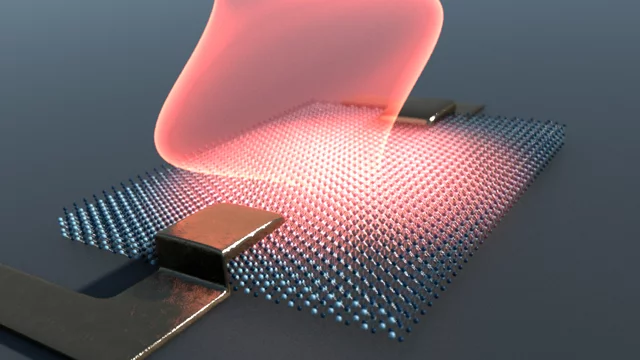
Imaging electrical switching of ultraefficient memory devices
SLS illuminates how electrical switching in layered materials works