  • Paul Scherrer Institut PSI
  • PSI Research, Labs & User Services

Digital User Office

  • Digital User Office
  • DE
  • EN
  • FR
Paul Scherrer Institut (PSI)
Search
Paul Scherrer Institut (PSI)

Hauptnavigation

  • Research at PSIOpen mainmenu item
    • Research Initiatives
    • Ethics and Research integrity
    • Scientific Highlights
    • Scientific Events
    • Scientific Career
    • PSI-FELLOW
    • PSI Data Policy
  • Research Divisions and LabsOpen mainmenu item
    • Overview
    • Research with Neutrons and Muons
    • Photon Science
    • Energy and Environment
    • Nuclear Energy and Safety
    • Biology and Chemistry
    • Scientific Computing, Theory and Data
    • Large Research Facilities
  • Facilities and InstrumentsOpen mainmenu item
    • Overview
    • Large Research Facilities
    • Facilities
    • PSI Facility Newsletter
  • PSI User ServicesOpen mainmenu item
    • User Office
    • Methods at the PSI User Facilities
    • Proposals for beam time
    • Proposal Deadlines
    • Data Analysis Service (PSD)
    • EU support programmes
  • New ProjectsOpen mainmenu item
    • SLS 2.0
    • IMPACT
  • DE
  • EN
  • FR

Digital User Office (mobile)

  • Digital User Office

You are here:

  1. PSI Home
  2. Labs & User Services
  3. NUM
  4. LMX
  5. Thin Films and Interfaces
  6. News & Highlights

Secondary navigation

Thin Films and Interfaces Group

  • About the TFI Group
    • Collaborations
    • Funding
  • People
    • Alumni
    • Visitors
  • Research
    • Thin Films - Methods
    • Plasma and Thin Film Analysis
    • Multiferroic Thin Films
    • Renewable Energy Applications
      • Ion Conductors
      • Thin Film Materials for Catalysis
    • Concluded Projects
      • Laser Induced Forward Transfer
      • Li-Metal Oxides
      • Structuring
      • Photo-Interactions with Polymers
    • Current Research Highlights
  • Instrumentation and Services
    • Instrumentation
      • Seifert Booking Page
    • Service for Industry
  • Seminars
    • Seminars 2022
    • Seminars 2021
    • Seminars 2020
    • Seminars 2019
    • Seminars 2018
    • Seminars 2017
    • Seminars 2016
    • Seminars 2015
    • Seminars 2014
    • Seminars 2013
    • Seminars 2012
    • Seminars 2011
    • Former Guest Speakers
  • Conferences
  • Teaching and Education
    • Micro- and Nanostructures
    • Inorganic Thin Films
    • Open Positions
  • News & Highlights Expanded submenu item
    • Highlights 2020
    • Highlights 2019
    • Highlights 2018
    • Highlights 2017
    • Highlights 2016
    • Highlights 2015
    • Highlights 2014
    • Highlights 2013
    • Highlights 2012
    • News
  • Publications
    • Papers
    • Books
    • PhD Theses
  • Useful links

  • Laboratory for Multiscale materials eXperiments
  • Laboratory for Neutron Scattering and Imaging
  • PSI Telefon Directory
  • Most Recent Publication
  • Student Projects

Scientific Highlights

Scientific Highlights

Toggle filters
Datum
1 August 2012

Laser-Induced Forward Transfer for the Fabrication of Devices

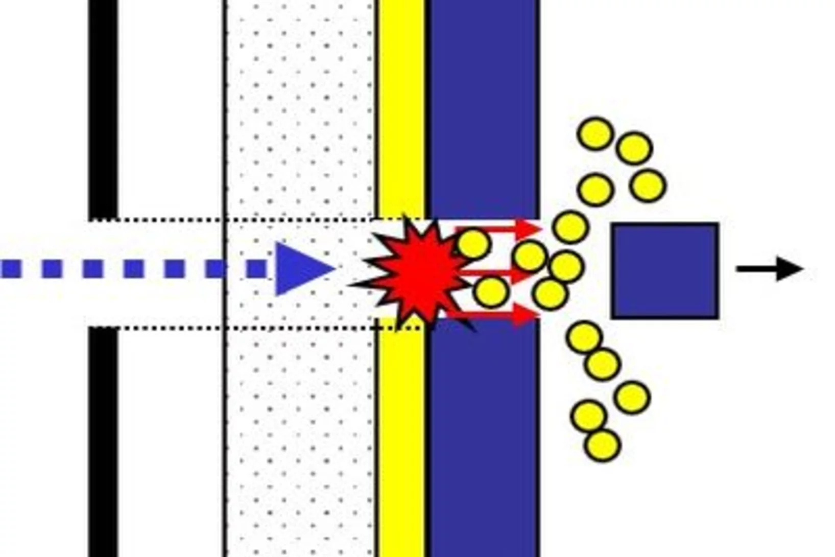
In conjunction with the increasing availability of cost-efficient laser units during the recent years, laser-based micromachining techniques have been developed as an indispensable industrial instrument of ‘‘tool-free’’ high-precision manufacturing techniques for the production of miniaturized devices made of nearly every type of materials. Laser cutting and drilling, as well as surface etching, have grown meanwhile to mature standard methods in laser micromachining applications where a well-defined laser beam is used to remove material by laser ablation. As an accurately triggerable nonmechanical tool, the ablating laser beam directly allows a subtractive direct-write engraving of precise microscopic structure patterns on surfaces, such as microchannels, grooves, and well arrays, as well as for security features. Therefore, laser direct-write (LDW) techniques imply originally a controlled material ablation to create a patterned surface with spatially resolved three-dimensional structures, and gained importance as an alternative to complementary photolithographic wet-etch processes. However, with more extended setups, LDW techniques can also be utilized to deposit laterally resolved micropatterns on surfaces, which allows, in a general sense, for the laser-assisted ‘‘printing’’ of materials.

Read more
3 July 2012
Room-temperature conductance of LASTO:x films for (a) x=0.50, (b) x=0.75, and (c) x=1. The dashed vertical lines for x=1.0 and 0.75 indicate the experimentally determined threshold thicknesses tc, which for x=0.5, is represented by a band for the more gradual transition. All values were obtained after ensuring that the samples had remained in dark conditions for a sufficiently long time to avoid any photoelectric contributions. The blue triangles are samples belonging to the first set, and red points denot…

Tunable conductivity threshold at polar oxide interfaces

The physical mechanisms responsible for the formation of a two-dimensional electron gas at the interface between insulating SrTiO3 and LaAlO3 have remained a contentious subject since its discovery in 2004. Opinion is divided between an intrinsic mechanism involving the build-up of an internal electric potential due to the polar discontinuity at the interface between SrTiO3 and LaAlO3, and extrinsic mechanisms attributed to structural imperfections.

Read more
27 June 2012

Sequential printing by laser-induced forward transfer to fabricate a polymer light-emitting diode pixel

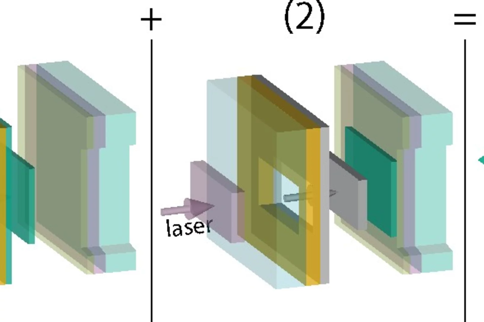
Patterned deposition of polymer light-emitting diode (PLED) pixels is a challenge for electronic display applications. PLEDs have additional problems requiring solvent orthogonality of different materials in adjacent layers. We present the fabrication of a PLED pixel by the sequential deposition of two different layers with laser-induced forward transfer (LIFT), a “dry” deposition technique. This novel use of LIFT has been compared to “normal” LIFT, where all the layers are transferred in a single step, and a conventional PLED fabrication process.

Read more
18 June 2012
(a) Mn K-edge XANES spectra of the ∼60 nm o-LMO epitaxial film were measured at room temperature for polarizations E || [110] and E || [001]. The inset shows the magnified pre-edge features. (b) FEFF simulations using the crystallographic data of the bulk o-LMO sample for E || [110] and E || [001]. The simulated pre-edges are shown on a larger scale in the inset.

Laser-Induced Forward Transfer for the Fabrication of Devices

X-ray near edge absorption spectroscopy was used to probe the electronic structure of multiferroic orthorhombic LuMnO3 polycrystalline samples and strained, twin-free orthorhombic (1–10) LuMnO3 films grown by pulsed laser deposition on (1–10) YAlO3 substrates. For all o-LuMnO3 samples x-ray near edge absorption spectroscopy spectra reveal that the pre-edge structure is influenced by the increase in MnO6 distortion as a result of the smaller Re-ion or film strain. Furthermore there is clear evidence of anisotropic Mn-O bonding and Mn orbital ordering along the c- and [110] direction. The experimental film and bulk data are in agreement with ab initio simulations.

Read more
15 May 2012
Summary of the LIFT process for tri-color OLED pixels. The 1-D substrate architecture is shown for the LIFT donor substrate (a) and the receiver substrate (b). The transfer of the first OLED color, blue, is shown in detail with the laser beam approaching (c) and the TP ablation and pixel deposition (d). LIFT of the green (e) and red (f) OLEDs is shown in sequence, and EL operation of the final three colors, side-by-side is also shown (g).

Red-green-blue polymer light-emitting diode pixels printed by optimized laser-induced forward transfer

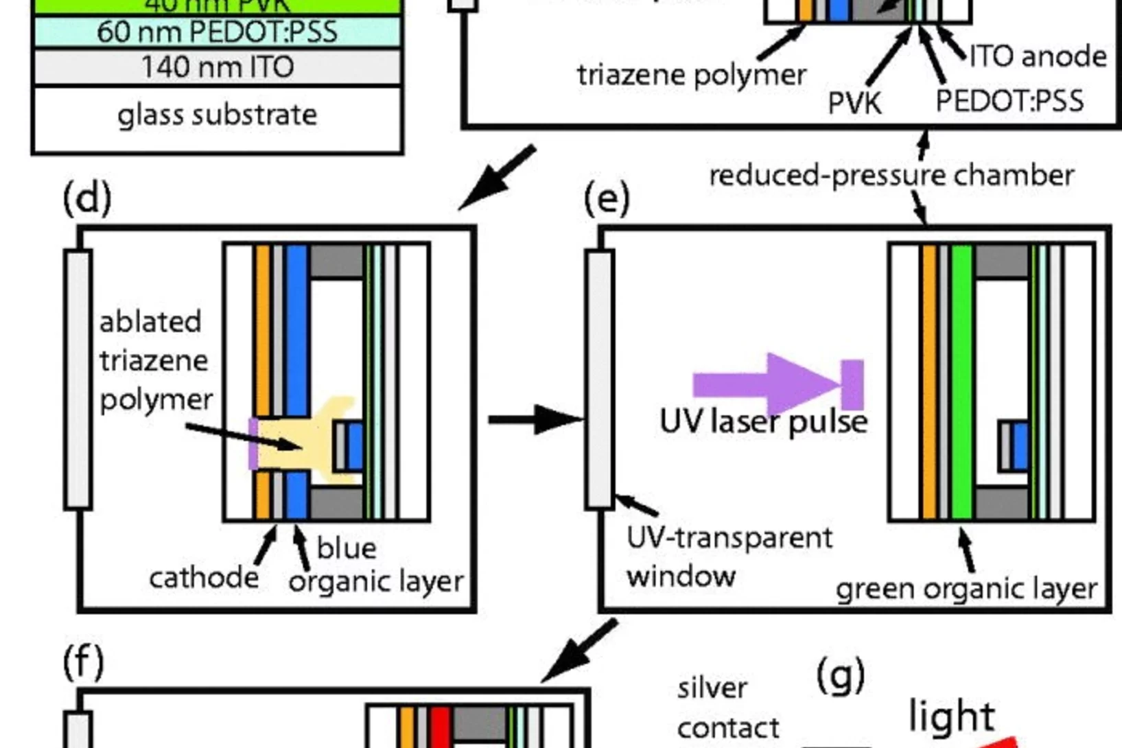
An optimized laser-induced forward transfer (LIFT) technique has been used to fabricate tri-color organic light-emitting diode (OLED) pixels. At reduced pressures, and with a defined donor-receiver gap, patterned depositions of polyfluorene-based OLED pixels have been achieved. OLED pixel functionality has been demonstrated and compared with devices made using conventional deposition techniques. In addition, improved functionality has been obtained by coating the cathode with an electron-injecting layer, a process not possible using conventional OLED fabrication techniques. The OLED pixels fabricated by LIFT reach efficiencies on the range of conventionally fabricated devices and even surpass them in the case of blue pixels.

Read more

Sidebar

Contact

Thin Films and Interfaces Group
Paul Scherrer Institut
5232 Villigen PSI
Switzerland
Homepage

Professor Dr. Dr. h.c. Thomas Lippert
Head of Group
OFLB/U110
tel: +41 56 310 4076
fax: +41 56 310 2688
thomas.lippert@psi.ch

Seminars

Thin Films and Interfaces Group Seminars
ENE Seminars
CMT seminar/journal club

Homepage NUM

Research with Neutrons and Muons NUM Division at PSI


PSI Scientific Reports

Archive 2006-2012. The Scientific Reports – containing accounts of research topics from all the different areas – provide an impression of the variety of subjects researched at PSI.


Scientific Advisory Committees

  • SINQ SAC
  • SμS SAC
  • CHRISP SAC
top

Footer

Paul Scherrer Institut

Forschungsstrasse 111
5232 Villigen PSI
Switzerland

Telephone: +41 56 310 21 11
Telefax: +41 56 310 21 99

How to find us
Contact

Visitor Centre psi forum
School Lab iLab (in German)
Center for Proton Therapy
PSI Education Centre
PSI Guest House
PSI Gastronomie (in German)
psi forum shop

Service & Support

  • Phone Book
  • User Office
  • Accelerator Status
  • PSI Publications
  • Suppliers
  • E-Billing
  • Computing
  • Safety (in German)

Career

  • Working at PSI
  • Job Opportunities
  • Training and further education
  • Career Center
  • Vocational Training (in German)
  • PSI Education Center

For the media

  • PSI in brief
  • Facts and Figures
  • Media corner
  • Media Releases
  • Social Media

Follow us: Twitter (in English) LinkedIn Youtube Facebook Instagram Issuu RSS

Footer legal

  • Imprint
  • Terms and Conditions
  • Editors' login