• Paul Scherrer Institut PSI
  • PSI Research, Labs & User Services

Digital User Office

  • Digital User Office
  • DE
  • EN
  • FR
Paul Scherrer Institut (PSI)
Suche
Paul Scherrer Institut (PSI)

Hauptnavigation

  • Research at PSIOpen mainmenu item
    • Research Initiatives
    • Research Integrity
    • Scientific Highlights
    • Scientific Events
    • Scientific Career
    • PSI-FELLOW
    • PSI Data Policy
  • Research Divisions and LabsOpen mainmenu item
    • Overview
    • Research with Neutrons and Muons
    • Photon Science
    • Energy and Environment
    • Nuclear Energy and Safety
    • Biology and Chemistry
    • Large Research Facilities
  • Facilities and InstrumentsOpen mainmenu item
    • Overview
    • Large Research Facilities
    • Facilities
    • PSI Facility Newsletter
  • PSI User ServicesOpen mainmenu item
    • User Office
    • Methods at the PSI User Facilities
    • Proposals for beam time
    • Proposal Deadlines
    • Data Analysis Service (PSD)
    • EU support programmes
  • DE
  • EN
  • FR

Digital User Office (mobile)

  • Digital User Office

You are here:

  1. PSI Home
  2. Labs & User Services
  3. PSD
  4. LMN
  5. Research Groups
  6. X-ray Optics (Old)
  7. Diamond: a gem for micro-optics

Secondary navigation

Laboratory for Micro and Nanotechnology

  • About LMN
    • Organisational Structure
  • Open Positions
  • People
  • Research Groups Expanded submenu item
    • Nanotechnology
    • X-ray Optics and Applications
      • X-ray Optics for Imaging and Spectroscopy
        • Fresnel Zone Plate for X-ray Microscopy
        • Blazed X-ray Optics
        • Zernike X-ray Phase Contrast Microscopy
        • Fresnel Zone Plates for RIXS
        • Refractive Lenses by 2 Photon 3D Lithography
      • Wavefront Metrology and Manipulation
        • Vortex Fresnel Zone Plates
        • Grating-based Wavefront Metrology
      • X-ray Optics for XFELs
        • Diamond Fresnel Zone Plates
        • Beam Splitter Gratings for Spectral Monitoring
        • A Delay Line for Ultrafast Pump-Probe Experiments
        • X-ray Streaking for Ultrafast Processes
    • Polymer Nanotechnology
      • Nanoimprint Lithography
      • Three Dimensional Structures
    • Molecular Nanoscience
      • On-surface Chemistry
      • Spins in Molecular Monolayers
      • SiC: Surfaces and Interfaces
      • Our Research Team
    • Advanced Lithography and Metrology
      • EUV Interference Lithography
      • EUV Lensless Imaging
      • ALM Nanoscience
    • Quantum Technologies
      • News and highlights
      • People
      • Open positions
      • Current projects
        • 2D semiconductor devices
        • CDW-based memory devices
        • Imaging quantum many-body states
        • Nonlinear magnonics
        • Rare-earth quantum magnets
        • Strained Germanium laser
      • Techniques
        • Cristallina-Q
        • IR beamline
        • Nano-fabrication
      • Publications
      • QTC@PSI
  • Facilities and Equipment
    • Cleanroom Labs
    • Surface Science Lab
    • Scanning Electron Microscopy
    • Scanning Probe Microscopy
    • PEARL Beamline
    • XIL Facility at the SLS
    • Nanoimprint Facilities
    • Electron Beam Lithography
  • LMN News
  • LMN Highlights
    • Archive
  • Publications
    • Publications 2011 - 2016
7 September 2018

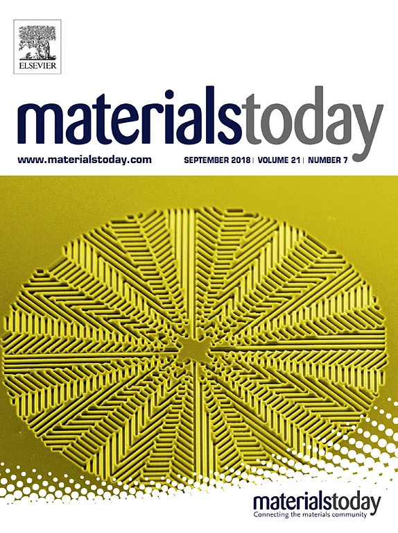
Diamond: a gem for micro-optics

Cover Page of the September 2018 issue of Materials Today

A lot of research in photonics is being directed towards optics miniaturization and light field control at the microscale. The concept of metasurfaces has proved to be highly efficient to engineer arbitrary light fields. Nevertheless, the performance of optical components still highly depends on their material properties, thus various compositions are being investigated to reduce loses and assure stable performance over a broad range of operation conditions. Low absorption, high refractive index, high threshold of radiation damage and thermal stability are greatly desired features. All these properties are well combined in diamond. Being extraordinarily hard and chemically inert diamond withstands harsh environments and aging. The large band gap makes it appear crystal clear and highly transparent from the UV to the far infrared bands. In addition, high refractive index at visible wavelengths and ultimate thermal conductivity prove diamond to be the material of choice. However, its hardness makes fabrication of micro-optical elements challenging.

Combination of electron beam lithography (EBL) and oxygen plasma etching is a possible way to pattern diamond. By using these techniques, we have successfully developed diamond micro-optical elements for the visible domain. As EBL patterning is in principle lateral, the desired optical functionalities are encoded by creating form birefringence domains. The domains consist of subwavelength gratings that act as waveplates for light field manipulation. As an example, vortex beam micro-generators of arbitrary topological charges were made by creating azimuthally varying subwavelength grating structure in diamond. The design of this structure benefits from the spin-orbit interaction of light, which converts a circularly polarized Gaussian beam into a vortex beam carrying an orbital angular momentum defined by the structure of micro-generator. Such elements provide high purity broadband optical vortex beams in the visible domain for a variety of applications in optical manipulation, microscopy and optical communications.

Original Publication

G. Seniutinas, E. Brasselet, A. Balčytis, C. David, S. Juodkazis
Diamond: a gem for micro-optics
Materials Today 21, 7, (2018) 798-799.

Sidebar

Contact

Dr. Christian David

Laboratory for Micro-
and Nanotechnology
Paul Scherrer Institut
5232 Villigen PSI
Switzerland

Telephone: +41 56 310 3753
Telefax: +41 56 310 2646
E-mail: christian.david@psi.ch

top

Footer

Paul Scherrer Institut

Forschungsstrasse 111
5232 Villigen PSI
Switzerland

Telephone: +41 56 310 21 11
Telefax: +41 56 310 21 99

How to find us
Contact form

Visitor Centre psi forum
School Lab iLab (in German)
Center for Proton Therapy
PSI Education Centre
PSI Guest House
PSI Gastronomie (in German)


Service & Support

  • Phone Book/People Search
  • User Office
  • Accelerator Status
  • PSI Publications
  • Suppliers
  • E-Billing
  • Computing
  • Safety (in German)

Career

  • Working at PSI
  • Job Opportunities
  • Training and further education
  • Vocational Training (in German)
  • PSI Education Center

For the media

  • PSI in brief
  • Facts and Figures
  • Media Contact
  • Media Releases
  • Social Media Newsroom

Follow us: Twitter (in English) LinkedIn Youtube Issuu RSS

Footer legal

  • Imprint
  • Terms and Conditions
  • Editors' login