• DE
  • EN
  • FR
Paul Scherrer Institut (PSI) Paul Scherrer Institut (PSI)
Suche
Paul Scherrer Institut (PSI) Paul Scherrer Institut (PSI)

Hauptnavigation

  • Labs & User ServicesOpen mainmenu item
    • Overview
    • Research at PSI
    • Research Divisions and Labs
    • Facilities and Instruments
    • Research Initiatives
    • PSI User Labs
    • Scientific Highlights
    • Scientific Events
    • Scientific Career
    • Useroffice
  • VisitorsOpen mainmenu item
    • Overview
    • Contact
    • How to find us
    • Public Events
    • Visitor Centre psi forum
    • Schülerlabor iLab
    • Center for Proton Therapy
  • IndustryOpen mainmenu item
    • Overview
    • Technology Transfer
    • Spin-off Companies
    • PARK innovAARE
  • Our ResearchOpen mainmenu item
    • Current topics from our research
    • Matter and Material
    • Human Health
    • Energy and Environment
    • Large Research Facilities
    • Brochures
    • Films
    • Media Corner
  • Career & Further EducationOpen mainmenu item
    • Job Opportunities
    • Personnel Policy
    • Working at PSI
    • Equal Opportunities, Diversity & Inclusion
    • Training and Further Education
    • Vocational Training
    • PSI Education Centre
    • Support Program "PSI Career Return Program"
    • PSI-FELLOW/COFUND
  • About PSIOpen mainmenu item
    • PSI in brief
    • Strategy
    • Guiding principles
    • Facts and figures
    • Organisational structure
    • Suppliers and customers
    • Customers E-Billing
    • IT and Computing
    • Safety at PSI (in German)

You are here:

  1. PSI Home
  2. Labs & User Services
  3. PSD
  4. LMN
  5. Research Groups
  6. SwissFEL nanoengineering
  7. Vacuum Nanoelectronics
  8. Laser induced emission

Secondary navigation

Laboratory for Micro and Nanotechnology

  • About LMN
    • Organisational Structure
  • Open Positions
  • People
  • Research Groups Expanded submenu item
    • Nanotechnology
    • X-ray Optics and Applications
      • X-ray Optics for Imaging and Spectroscopy
        • Fresnel Zone Plate for X-ray Microscopy
        • Blazed X-ray Optics
        • Zernike X-ray Phase Contrast Microscopy
        • Fresnel Zone Plates for RIXS
        • Refractive Lenses by 2 Photon 3D Lithography
      • Wavefront Metrology and Manipulation
        • Vortex Fresnel Zone Plates
        • Grating-based Wavefront Metrology
      • X-ray Optics for XFELs
        • Diamond Fresnel Zone Plates
        • Beam Splitter Gratings for Spectral Monitoring
        • A Delay Line for Ultrafast Pump-Probe Experiments
        • X-ray Streaking for Ultrafast Processes
    • Polymer Nanotechnology
      • Nanoimprint Lithography
      • Three Dimensional Structures
    • Molecular Nanoscience
      • On-surface Chemistry
      • Spins in Molecular Monolayers
      • SiC: Surfaces and Interfaces
      • Our Research Team
    • Advanced Lithography and Metrology
      • EUV Interference Lithography
      • EUV Lensless Imaging
      • ALM Nanoscience
    • Quantum Technologies
      • News and highlights
      • People
      • Open positions
      • Current projects
        • 2D semiconductor devices
        • CDW-based memory devices
        • Imaging quantum many-body states
        • Nonlinear magnonics
        • Rare-earth quantum magnets
        • Strained Germanium laser
      • Techniques
        • Cristallina-Q
        • IR beamline
        • Nano-fabrication
      • Publications
      • QTC@PSI
  • Facilities and Equipment
    • Cleanroom Labs
    • Surface Science Lab
    • Scanning Electron Microscopy
    • Scanning Probe Microscopy
    • PEARL Beamline
    • XIL Facility at the SLS
    • Nanoimprint Facilities
    • Electron Beam Lithography
  • LMN News
  • LMN Highlights
    • Archive
  • Publications
    • Publications 2011 - 2016

Ultrafast near infrared laser-induced field emission

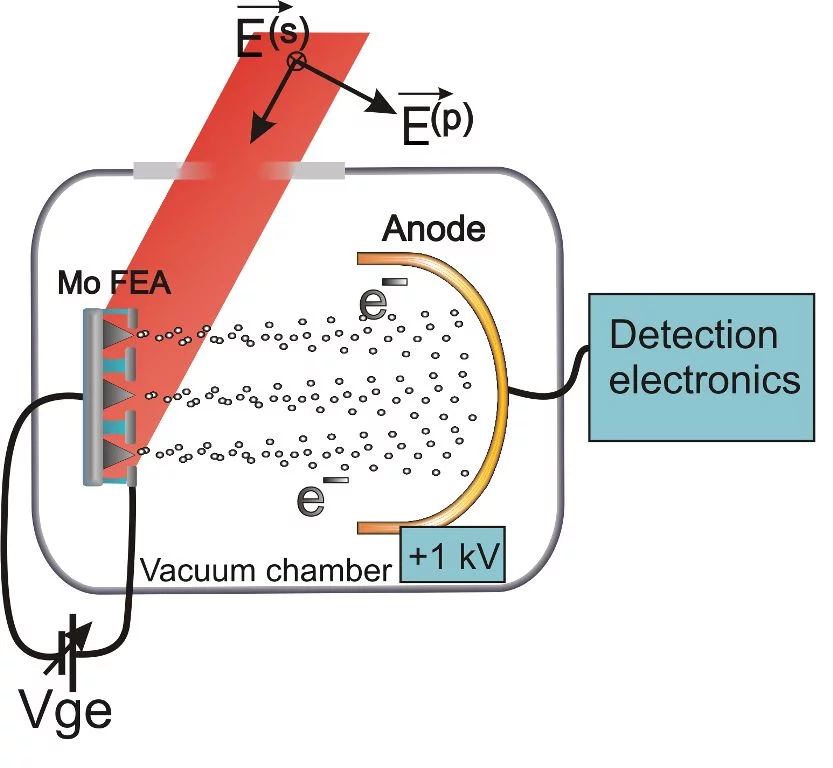
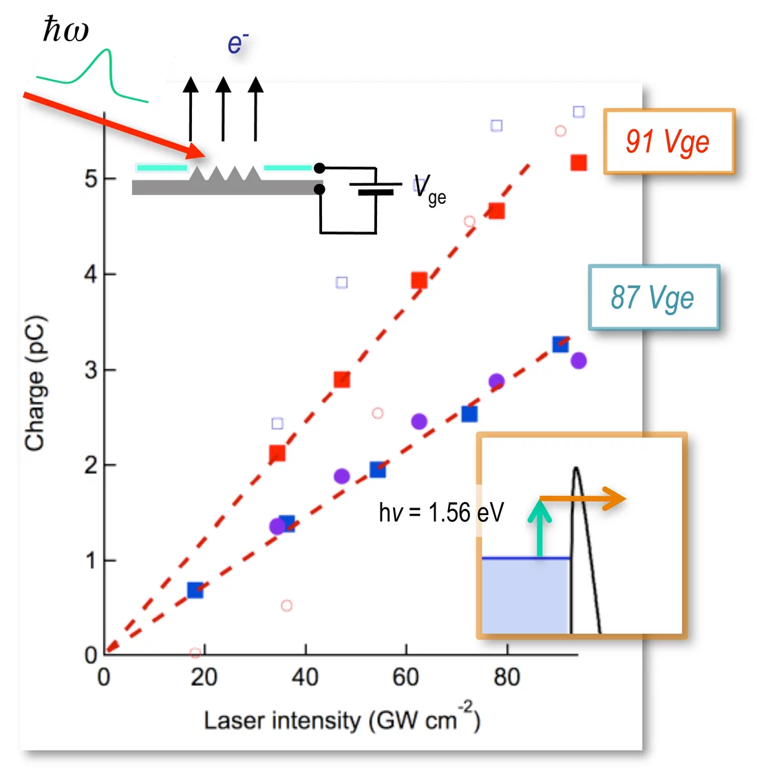
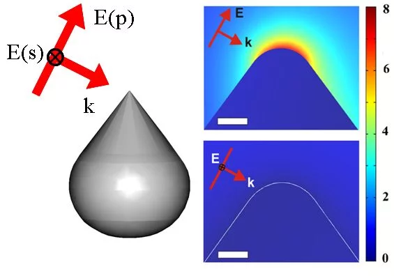
Ultrafast electron pulses can be produced from sharp metallic tips illuminated by femtosecond near infrared laser pulses [1-3]; generation of ~5 pC from 120k-tip single-gate molybdenum FEA with 5 um pitch emitters by near infrared laser pulses was demonstrated recently, showing that the use of an array of metallic nanotips for high charge bunch generation and accelerator applications is also feasible but the small fraction of the emitter tip area limits the quantum efficiency. In a recent work, we are developing a submicron-pitch, high-density nanotip array device with a gate electrode [4-6], that can support surface-plasmon polaritons. From a theoretical analysis for a device with an asymmetric emitter position, a factor ~30 increased array quantum efficiency, within a factor of 60 in comparison with the UV-excited Copper photocathode, is demonstrated [4].
Fig.1 Laser-induced field emission experiment
Fig.2 Laser intensity dependence of generated electron bunch charge

Fig.3 Enhancement of optical electic field at the metallic nano-tip: simulation

We further investigated theoretically the laser-induced field emission from stacked-double gate devices, to explore the potential of such system to generate collimated field emission beams [4,7]. Using electromagnetic and particle tracking simulations, we showed that electron pulses with small rms transverse velocities are eciently produced from nanotip arrays by laser-induced field emission with the laser wavelength tuned to surface plasmon polariton resonance of the stacked double-gate structure. The result indicates the possibility of realizing a metal nanotip array cathode that outperforms state-of-the-art photocathodes.
Fig.4 Generation of collimated electron beams by near infrared laser-induced field emission from metallic nano-tip arrays: resonant enhancement of the laser-tip interaction via surface plasmon polariton resonance and collimation of the field emission beams by the on-chip stacked double-gate structure[4,7]

References

[1] S. Tsujino, P. Beaud, E. Kirk, T. Vogel, H. Sehr, J. Gobrecht, and A. Wrulich Ultrafast electron emission from metallic nanotip arrays induced by near infrared femtosecond laser pulses, Appl. Phys. Lett. 92, 193501 (2008); Selected in Virtual Journal of Ultrafast Science -- June 2008, Volume 7, Issue 6.

[2] S. Tsujino, F. le Pimpec, J. Raabe, M. Buess, M. Dehler, E. Kirk, J. Gobrecht, and A. Wrulich, Static and optical field enhancement in metallic nanotips studied by two-photon photoemission microscopy and spectroscopy excited by picosecond laser pulses, Appl. Phys. Lett. 94, 093508 (2009); Selected for the March 16, 2009 issue of Virtual Journal of Nanoscale Science & Technology; Selected for April 2009 issue (Volume 8, Issue 4) of Virtual Journal of Ultrafast Science.

[3] A. Mustonen, P. Beaud, E. Kirk, T. Feurer, and S. Tsujino, Five picocoulomb electron bunch generation by ultrafast laser-induced field emission from metallic nano-tip arrays, Appl. Phys. Lett. 99, 103504 (2011); Selected for September 19, 2011 issue (Volume 24, Issue 12) of Virtual Journal of Nanoscale Science & Technology; Selected for October 2011 issue (Volume 10, Issue 10) of Virtual Journal of Ultrafast Science; highlighted in Nature Photonics, 5, 644-645 (November 2011).

[4] A. Mustonen, P. Beaud, E. Kirk, T. Feurer, and S. Tsujino, Efficient light coupling for optically excited high-density metallic nanotip arrays, Scientific Reports, 2, 915 (2012).

[5] A. Mustonen, V. Guzenko, C. Spreu, T. Feurer, and S. Tsujino, High-density metallic nano-emitter arrays and their field emission characteristics, Nanotechnology 25, 085203 (2014).

[6] V. Guzenko, A. Mustonen, P. Helfenstein, E. Kirk, and S. Tsujino, High-density large-scale field emitter arrays for X-ray free electron laser cathodes, Microelectronic Engineering (2013).

[7] P. Helfenstein, A. Mustonen, T. Feurer, and S. Tsujino, Collimated Field Emission Beams from Metal Double-Gate Nanotip Arrays Optically Excited via Surface Plasmon Resonance, Applied Physics Express 6, 114301 (2013). .


Sidebar

Contact

Dr. Soichiro Tsujino

Paul Scherrer Institut
5232 Villigen PSI
Switzerland

Telephone:
+41 56 310 2304
Telefax:
+41 56 310 2646
E-mail:
soichiro.tsujino@psi.ch

IVNC2020

The 33th International Vacuum Nanoelectronics Conference (IVNC 2020) in Virtual, 6-8, July 2020;


top

Footer

Paul Scherrer Institut

Forschungsstrasse 111
5232 Villigen PSI
Switzerland
How to find us

Imprint
Terms and Conditions

Login

Telephone: +41 56 310 21 11
Telefax: +41 56 310 21 99
Contact form

Visitor Centre psi forum
School Lab iLab (in German)
Center for Proton Therapy

Follow us: Twitter (in English) LinkedIn Youtube Issuu RSS

Quicklinks

  • Phone Book/People Search
  • Digital User Office
  • Technology transfer
  • PSI Publications
  • Computing
  • Safety (in German)
  • Job Opportunities
  • Vocational Training (in German)
  • Suppliers
  • Customers E-Billing
  • PSI Guest House
  • PSI Gastronomie (in German)

For the media

  • Media Contact
  • Media Releases
  • Social Media Newsroom
  • Facts and Figures
  • PSI in brief
  • Films
  • DE
  • EN
  • FR