• DE
  • EN
  • FR
Paul Scherrer Institut (PSI) Paul Scherrer Institut (PSI)
Suche
Paul Scherrer Institut (PSI) Paul Scherrer Institut (PSI)

Hauptnavigation

  • Labs & User ServicesOpen mainmenu item
    • Overview
    • Research at PSI
    • Research Divisions and Labs
    • Facilities and Instruments
    • Research Initiatives
    • PSI User Labs
    • Scientific Highlights
    • Scientific Events
    • Scientific Career
    • Useroffice
  • VisitorsOpen mainmenu item
    • Overview
    • Contact
    • How to find us
    • Public Events
    • Visitor Centre psi forum
    • Schülerlabor iLab
    • Center for Proton Therapy
  • IndustryOpen mainmenu item
    • Overview
    • Technology Transfer
    • Spin-off Companies
    • PARK innovAARE
  • Our ResearchOpen mainmenu item
    • Current topics from our research
    • Matter and Material
    • Human Health
    • Energy and Environment
    • Large Research Facilities
    • Brochures
    • Films
    • Media Corner
  • Career & Further EducationOpen mainmenu item
    • Job Opportunities
    • Personnel Policy
    • Working at PSI
    • Equal Opportunities, Diversity & Inclusion
    • Training and Further Education
    • Vocational Training
    • PSI Education Centre
    • Support Program "PSI Career Return Program"
    • PSI-FELLOW/COFUND
  • About PSIOpen mainmenu item
    • PSI in brief
    • Strategy
    • Guiding principles
    • Facts and figures
    • Organisational structure
    • Suppliers and customers
    • Customers E-Billing
    • IT and Computing
    • Safety at PSI (in German)

You are here:

  1. PSI Home
  2. Labs & User Services
  3. PSD
  4. LMN
  5. Research Groups
  6. SwissFEL nanoengineering
  7. Vacuum Nanoelectronics
  8. Double gated FEAs

Secondary navigation

Laboratory for Micro and Nanotechnology

  • About LMN
    • Organisational Structure
  • Open Positions
  • People
  • Research Groups Expanded submenu item
    • Nanotechnology
    • X-ray Optics and Applications
      • X-ray Optics for Imaging and Spectroscopy
        • Fresnel Zone Plate for X-ray Microscopy
        • Blazed X-ray Optics
        • Zernike X-ray Phase Contrast Microscopy
        • Fresnel Zone Plates for RIXS
        • Refractive Lenses by 2 Photon 3D Lithography
      • Wavefront Metrology and Manipulation
        • Vortex Fresnel Zone Plates
        • Grating-based Wavefront Metrology
      • X-ray Optics for XFELs
        • Diamond Fresnel Zone Plates
        • Beam Splitter Gratings for Spectral Monitoring
        • A Delay Line for Ultrafast Pump-Probe Experiments
        • X-ray Streaking for Ultrafast Processes
    • Polymer Nanotechnology
      • Nanoimprint Lithography
      • Three Dimensional Structures
    • Molecular Nanoscience
      • On-surface Chemistry
      • Spins in Molecular Monolayers
      • SiC: Surfaces and Interfaces
      • Our Research Team
    • Advanced Lithography and Metrology
      • EUV Interference Lithography
      • EUV Lensless Imaging
      • ALM Nanoscience
    • Quantum Technologies
      • News and highlights
      • People
      • Open positions
      • Current projects
        • 2D semiconductor devices
        • CDW-based memory devices
        • Imaging quantum many-body states
        • Nonlinear magnonics
        • Rare-earth quantum magnets
        • Strained Germanium laser
      • Techniques
        • Cristallina-Q
        • IR beamline
        • Nano-fabrication
      • Publications
      • QTC@PSI
  • Facilities and Equipment
    • Cleanroom Labs
    • Surface Science Lab
    • Scanning Electron Microscopy
    • Scanning Probe Microscopy
    • PEARL Beamline
    • XIL Facility at the SLS
    • Nanoimprint Facilities
    • Electron Beam Lithography
  • LMN News
  • LMN Highlights
    • Archive
  • Publications
    • Publications 2011 - 2016

Stacked double-gate field emitter arrays with large collimation gate apertures

Double-gate field emitter array equipped with a collimation gate electrode for the individual emitters in addition to an electron extraction gate electrode can reduce the rms transverse electron veloecy of the field emission beamlet and the emittance of the FEA beam. We have shown recently that an order of magnitude reduction of the rms transverse electron velocity can be achieved with our structure with minimal reduction of the emission current [1,2,3,4]. Further effort to match the cathode spec [5,6] for the SwissFEL X-ray free electron laser [7] is under way.
Double-gate FEA with 40'000 tips with 2 mm diameter. (Left) Overview, (Right) Closeup of a small part of the FEA and a single emitter
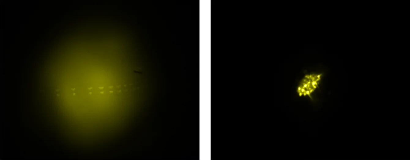
FIeld emission beam generated by double-gate FEA. (Left) Uncollimated beam. (Right) Collimated beam (small spots show x10 collimated beamlets from separate emitters
Although high current FEAs have been intensively studied to realize a compact vacuum electronic amplifier, such as traveling wave tubes (TWTs) [8,9,10], and working FEA-TWT in 5 GHz range with 100 W output have been already demonstrated [10], double-gate FEAs with low normalized emittance will be essential to fully take advantage of the high current density characteristic of FEAs, in particular for the compact THz amplifiers [11,12] and THz power modules (a the vacuum electronic amplifiers seeded by solid-state low-power oscillators) [e.g. 13]. These FEAs may also be applicable for the massively parallel electron beam lithography tools [e.g. 14].

References

[1] S. Tsujino, P. Helfenstein, E. Kirk, T. Vogel, C. Escher, and H.-W. Fink, Field-emission characteristics of molded molybdenum nanotip arrays with stacked collimation gate electrodes, IEEE Electron Device Letters, vol. 31, 1059 (2010).

[2] P. Helfenstein, E. Kirk, K. Jefimovs, T. Vogel, C. Escher, H.-W. Fink, and S. Tsujino, Highly collimated electron beams from double-gate field emitter arrays with large collimation gate apertures, Appl. Phys. Lett. 98, 061502 (2011).

[3] P. Helfenstein, K. Jefimovs, E. Kirk, C. Escher, H.-W. Fink, and S. Tsujino, Fabrication of metallic double-gate field emitter arrays and their electron beam collimation characteristics, J. Appl. Phys. 112, 093307 (2012).

[4] P. Helfenstein, V. A. Guzenko, H.-W. Fink, and S. Tsujino, Electron beam collimation with a 40 000 tip metallic double-gate field emitter array and in-situ control of nanotip sharpness distribution, J. Appl. Phys. 113, 043306 (2013).

[5] M. Dehler, A. Candel, E. Gjonaj, Full scale simulation of a field-emitter arrays based electron source for free-electron lasers, J. Vac. Sci. Tech. B 24,892-897 (2006).

[6] M. Dehler, Design and modeling of field emitter arrays for a high brilliance electron source, Proceedings of the 9th International Computational Accelerator Physics Conference (ICAP2006), (Chamonix, France, 2-6, Oct. 2006).

[7] B. Patterson, R. Abela, H.-H. Braun, U. Flechsig, R. Ganter, Y. Kim, E. Kirk, A. Oppelt, M. Pedrozzi, S. Reiche, L. Rivkin, Th. Schmidt, B. Schmidt, V. N. Strocov, S. Tsujino, and A. F. Wrulich, New J. Physics, 12, 035012 (2010).

[8] H. Makishima, S. Miyano, H. Imura, J. Matsuoka, H. Takemura, and A. Okamoto, Design and performance of traveling-wave tubes using field emitter array cathodes, Appl. Surf. Sci. 146, 230 (1999).

[9] D.R. Whaley, B.M. Gannon, C.R. Smith, C.M. Armstrong, and C.A. Spindt, Application of field emitter arrays to microwave power amplifiers, IEEE Trans. Plasma Sci. 28, 727 (2000).

[10] D.R. Whaley, R. Duggal, C.M. Armstrong, C.L. Bellew, C.E. Holland, and C.A. Spindt, 100 W Operation of a cold cathode TWT, IEEE Trans. ED 56, 896 (2009).

[11] H. Booske, Plasma physics and relate challenges of millimeter-wave-to-terahertz and high power microwave generation, Phys. Plasmas 15, 055502 (2008).

[12] R.L. Ives, Microfabrication of high-frequency vacuum electron devices, IEEE Trans. Plasma Sci. 32, 1277 (2004).

[13] J. Tucek, M. Basten, D. Gallagher, K. Kreischer, R. Lai, V. Radisic, and K. Leong, A 100 mW, 0.670 THz power module, Proceedings of the IVEC-IVESC 2012, Montrey, CA, 24-26, April, 2012.

[14] E. Platzgummer, C. Klein, and H. Loeschner, Results of proof-of-concept 50 keV electron multi-beam mask exposure tool (eMET POC), Proceedings of Photomask Japan (PMJ) 2012, Yokohama, Japan.

Sidebar

Contact

Dr. Soichiro Tsujino

Paul Scherrer Institut
5232 Villigen PSI
Switzerland

Telephone:
+41 56 310 2304
Telefax:
+41 56 310 2646
E-mail:
soichiro.tsujino@psi.ch

IVNC2020

The 33th International Vacuum Nanoelectronics Conference (IVNC 2020) in Virtual, 6-8, July 2020;


top

Footer

Paul Scherrer Institut

Forschungsstrasse 111
5232 Villigen PSI
Switzerland
How to find us

Imprint
Terms and Conditions

Login

Telephone: +41 56 310 21 11
Telefax: +41 56 310 21 99
Contact form

Visitor Centre psi forum
School Lab iLab (in German)
Center for Proton Therapy

Follow us: Twitter (in English) LinkedIn Youtube Issuu RSS

Quicklinks

  • Phone Book/People Search
  • Digital User Office
  • Technology transfer
  • PSI Publications
  • Computing
  • Safety (in German)
  • Job Opportunities
  • Vocational Training (in German)
  • Suppliers
  • Customers E-Billing
  • PSI Guest House
  • PSI Gastronomie (in German)

For the media

  • Media Contact
  • Media Releases
  • Social Media Newsroom
  • Facts and Figures
  • PSI in brief
  • Films
  • DE
  • EN
  • FR