• Paul Scherrer Institut PSI
  • PSI Research, Labs & User Services

Digital User Office

  • Digital User Office
  • DE
  • EN
  • FR
Paul Scherrer Institut (PSI)
Search
Paul Scherrer Institut (PSI)

Hauptnavigation

  • Research at PSIOpen mainmenu item
    • Research Initiatives
    • Ethics and Research integrity
    • Scientific Highlights
    • Scientific Events
    • Scientific Career
    • PSI-FELLOW
    • PSI Data Policy
  • Research Divisions and LabsOpen mainmenu item
    • Overview
    • Research with Neutrons and Muons
    • Photon Science
    • Energy and Environment
    • Nuclear Energy and Safety
    • Biology and Chemistry
    • Scientific Computing, Theory and Data
    • Large Research Facilities
  • Facilities and InstrumentsOpen mainmenu item
    • Overview
    • Large Research Facilities
    • Facilities
    • PSI Facility Newsletter
  • PSI User ServicesOpen mainmenu item
    • User Office
    • Methods at the PSI User Facilities
    • Proposals for beam time
    • Proposal Deadlines
    • Data Analysis Service (PSD)
    • EU support programmes
  • New ProjectsOpen mainmenu item
    • SLS 2.0
    • IMPACT
  • DE
  • EN
  • FR

Digital User Office (mobile)

  • Digital User Office

You are here:

  1. PSI Home
  2. Labs & User Services
  3. PSD
  4. LNQ
  5. Research Groups
  6. Advanced Nanomanufacturing
  7. Research Projects
  8. Three Dimensional Structures

Secondary navigation

Laboratory for Nano and Quantum Technologies

  • About LNQ
    • Organisational Structure
  • People
  • Research Groups Expanded submenu item
    • Nanotechnology Group
      • People
      • Research Projects
    • Quantum Engineering
      • People
      • Research Projects
    • Advanced Nanomanufacturing Expanded submenu item
      • People
      • Research Projects Expanded submenu item
        • Three dimensional surface topographies
        • Nanoimprint Lithography
      • Scientific Highlights and News
    • Superconducting Quantum Circuits Group
      • People
      • Scientific Highlights and News
    • Bosonic Quantum Information
      • People
      • Open positions
      • Scientific Highlights and News
    • Ion Trap Quantum Computing
      • Open Positions
      • People
      • Publications
    • Photonics – INPhO
      • People
  • Facilities and Equipment
    • ETHZ-PSI Quantum Computing Hub
    • Cleanroom Laboratories
    • Nanoimprint Lithography Facilities
    • Scanning Electron Microscopy
  • Scientific Highlights and News
    • Archive
  • Publications

Three dimensional surface topographies

3D topographies are highly attractive for various applications in optics, fluidics, or biosciences, where a complex surface profile adds an improved functionality to elements or devices. However, current lithographies are often limited in pattern variety. Therefore structures are often fabricated using the combinations of different processes in a sequential way. Using grayscale lithography and selective thermal reflow, we are now able to fabricate patterns at the micro- and nanometer scale with different sizes, shapes, depths, and lateral extension on the same substrate as needed for various applications.

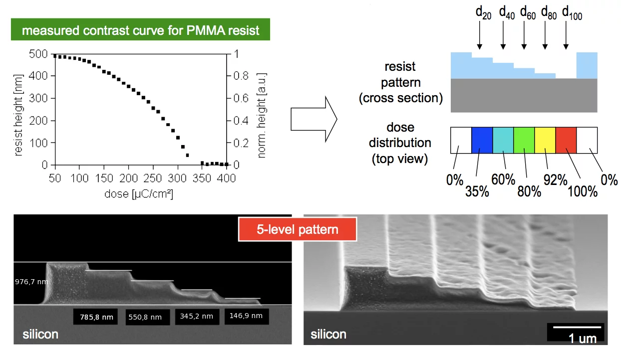
Contrast curve for dose-depth correlation in PMMA film and its application for a 5-level staircase structure.
Grayscale lithography Exposure with electrons modifies the molecular weight of the resist and thus its etching characteristics in a solvent. A 3D profile with different height levels can be generated by local dose-modulation. For this, a CAD design with different layers is generated, each respresenting a different resist level. To each layer a dose is assigned according to a constrast curve calibrated for a specific resist, developer and time. The final dose assignment is done with specialized programs using proximity correction.

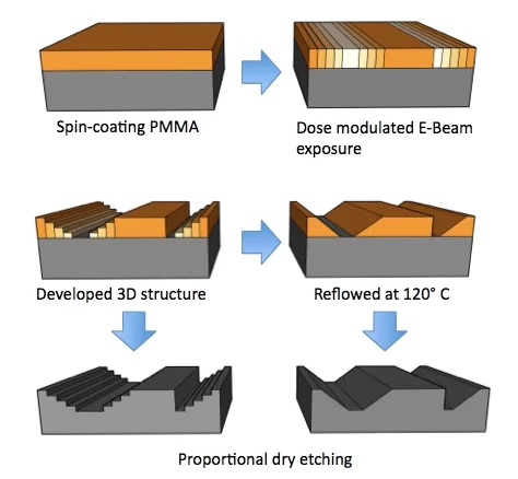
Process for 3D structure origination with stepped and sloped profiles and pattern transfer into a silicon substrate.

Selective thermal reflow During exposure, both the etch rate and the ability of the polymer to flow at a specific temperature are modified, enabling to etch different depths and to reflow these areas while those unexposed preserve their original shape. Therefore structures with both vertical and sloped sidewalls can be fabricated in the same resist. Further developments enable the fabrication of hybrid structures (surface nanostructures added before reflow) and combinations of processes (nanoimprint, exposure and reflow). This process is called TASTE (Thermally Assisted Selective Topography Equilibration). After pattern transfer these structures can be used as stamp for nanoimprint lithography and other replication techniques.

Reflow of polymer microsteps fabricated with grayscale lithography


Microsteps fabricated by dose dependent electron beam exposure (grayscale lithography) reflowed on a hotplate at 120° C over two hours.

Publications

Combining nanoimprint lithography and a molecular weight selective thermal reflow for the generation of mixed 3D structures
J. Vac. Sci. Technol. B 29 06FC01 (2011)
A. Schleunitz, C.Spreu, M. Vogler, H. Atasoy, H.Schift

Selective profile transformation of electron-beam exposed multilevel resist structures based on a molecular weight dependent thermal reflow
A. Schleunitz, V. Guzenko, A. Schander, M. Vogler, H. Schift
J. Vac. Sci. Technol. B 29, 06F302 (2011)

Fabrication of 3D nanoimprint stamps with continuous reliefs using dose-modulated electron beam lithography and thermal reflow
A. Schleunitz and H. Schift
J. Micromech. Microeng. 20 095002 (2010)


Sidebar

Contact

Dr. Helmut Schift

Laboratory for Micro-
and Nanotechnology
Paul Scherrer Institut
5232 Villigen PSI
Switzerland

Telephone: +41 56 310 2839
E-mail: helmut.schift@psi.ch

top

Footer

Paul Scherrer Institut

Forschungsstrasse 111
5232 Villigen PSI
Switzerland

Telephone: +41 56 310 21 11
Telefax: +41 56 310 21 99

How to find us
Contact

Visitor Centre psi forum
School Lab iLab (in German)
Center for Proton Therapy
PSI Education Centre
PSI Guest House
PSI Gastronomie (in German)
psi forum shop

Service & Support

  • Phone Book
  • User Office
  • Accelerator Status
  • PSI Publications
  • Suppliers
  • E-Billing
  • Computing
  • Safety (in German)

Career

  • Working at PSI
  • Job Opportunities
  • Training and further education
  • Career Center
  • Vocational Training (in German)
  • PSI Education Center

For the media

  • PSI in brief
  • Facts and Figures
  • Media corner
  • Media Releases
  • Social Media

Follow us: Twitter (in English) LinkedIn Youtube Facebook Instagram Issuu RSS

Footer legal

  • Imprint
  • Terms and Conditions
  • Editors' login