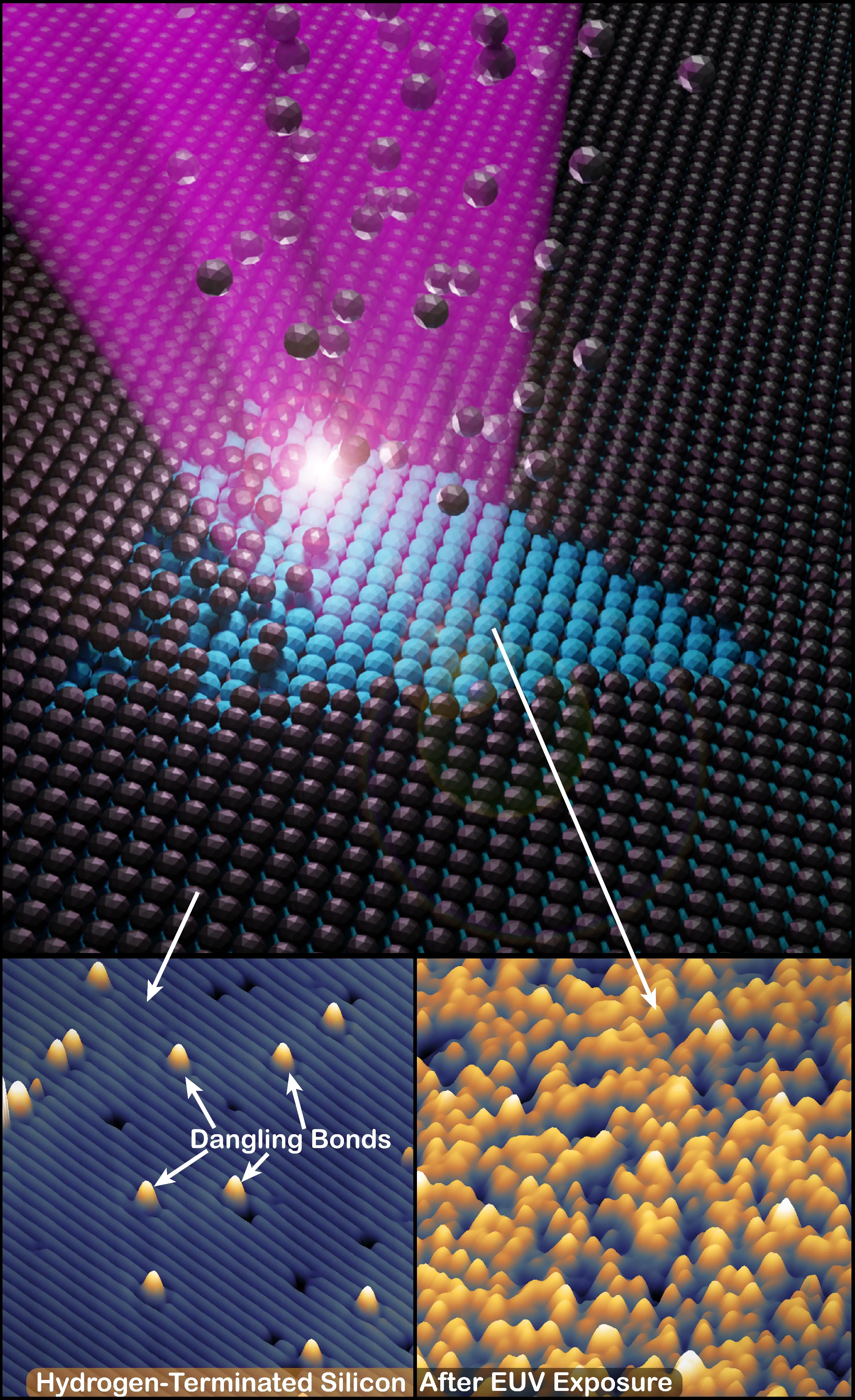
Extreme-ultraviolet light (EUV) is the key to state-of-the-art mass production of the classical electronics which drives the continuing information revolution. Scientists from PSI, UCL, EPFL and ETHZ have now used the Swiss Light Source (SLS) to perform the first experiments to demonstrate the potential of EUV for the manufacture of silicon-based quantum nanoelectronics, the building block for truly scalable quantum computers.
In the rapidly advancing domain of semiconductor technologies and quantum computing, scientists have developed methods to engineer devices at the atomic scale. Yet, the challenge of patterning large-scale devices remains a significant obstacle to scale-up, particularly when it comes to fabricating extensive arrays required for dopant-based qubits in silicon. One traditional method relies on the scanning tunnelling microscope (STM), where the high current density of electrons tunnelling from a sharp tip are used to pattern hydrogen-passivated silicon with an atomic-scale precision. But what if we could accomplish this feat using photons instead?
Photons, which are integral to high-volume semiconductor manufacturing through extreme ultra-violet (EUV) lithography, enable the patterning of arrays of billions of transistors to then yield high performance microprocessor, GPU or memory chips, thanks to the use of reflective masks. Now, a team of researchers led by Dr Procopios Constantinou from the Paul Scherrer Institute (PSI) and Associate Professor Steven Schofield from University College London (UCL) have demonstrated for the first time that hydrogen atoms can be desorbed from hydrogen-passivated silicon surfaces using EUV light instead of an STM. This ground-breaking research, published in Nature Communications, provides a path to patterning dopant atoms into silicon over large areas, bridging the gap between atomic-scale STM patterning and large-scale industrial semiconductor manufacturing.
The cutting-edge PEARL and SIM beamlines at the SLS proved critical to the success of these experiments
The PEARL beamline at the SLS provides comprehensive sample preparation, STM, and photoelectron spectroscopy (XPS), all within a single dedicated ultrahigh vacuum system. This powerful platform gave the UCL & PSI team exactly the combination of resources required for their groundbreaking experiments. The team prepared silicon crystals with a single atom thick layer of hydrogen atoms chemically attached to the surface. They then exposed the surface to x-ray light from the SLS to determine if can be used to remove hydrogen atoms from the surface. Using XPS, the team confirmed that after exposure, the surface exhibited the characteristic spectroscopic fingerprint of hydrogen-free silicon. Subsequently, they used STM, with its capability to directly image the individual atoms of the surface, to unequivocally demonstrate that hydrogen atoms were desorbed from the surface within the region exposed to the x-ray beam.
By varying the range of wavelengths used in the x-ray exposures, the researchers were able to establish that high energy photons in the EUV range are responsible for the hydrogen desorption and not low energy photons (< 10 eV), the latter of which are not so useful for nanoscale patterning given their long wavelengths (> 120 nm).
The team also quantified the desorption by examining how changes in the incident EUV power impact the desorption rate and were thereby able to deduce the physical mechanism responsible. An observed non-linear desorption rate was found to be a good fit to a model that suggests that the desorption is instigated by secondary electrons ejected from near-surface silicon atoms. This result suggests a likely spatial-patterning resolution limit of around 10 nm, although this is yet to be verified experimentally.
The hydrogen desorption experiment was repeated using the high brilliance SIM beamline at SLS, which provides the capability for real-space photoelectron imaging. Here, a rudimentary pattern was made and imaged, serving as a proof-of-principle for EUV-based patterning of hydrogen-terminated silicon for the creation of patterned dopant quantum devices.
Towards large-scale EUV patterning of silicon quantum devices
Given the use of EUV lithography at 13.5 nm (~92 eV) by industry leaders such as Samsung, Intel, and TSMC for 5 nm nodes and beyond, the authors demonstration that hydrogen can be desorbed from hydrogen-terminated silicon using EUV light presents a unifying link between industrial semiconductor processing and atomic-scale fabrication. The authors propose a programme of work at synchrotrons as well as commercial EUV lithography stations which could eventually enable the writing of the complex qubit and classical control architectures required for a truly useful quantum processor.
Now published in Nature Communications, this research represents a significant step forward which opens exciting new possibilities for the future of semiconductor technologies and quantum computing.
Text: PSI/UCL, Schofield, Constantinou, Aeppli
Contact
Dr Procopios Constantinou
Photon Science Division
Paul Scherrer Institut, 5232 Villigen PSI, Switzerland
Email: procopios.constantinou@psi.ch
Assoc. Prof. Dr. Steven R. Schofield
London Centre for Nanotechnology
University College London, London, WC1H 0AH, UK
Email: s.schofield@ucl.ac.uk
Prof. Dr. Gabriel Aeppli
Photon Science Division
Paul Scherrer Institut, 5232 Villigen PSI, Switzerland
Department of Physics & Quantum Center
Eidgenössische Technische Hochschule Zürich, 8093 Zürich, Switzerland
Institute of Physics
Ecole Polytechnique Fédérale de Lausanne, 1015 Lausanne, Switzerland
Email: aepplig@ethz.ch
Original Publication
"EUV-induced hydrogen desorption as a step towards large-scale silicon quantum device patterning" Procopios Constantinou, Taylor J. Z. Stock, Li-Ting Tseng, Dimitrios Kazazis, Matthias Muntwiler, Carlos A. F. Vaz, Yasin Ekinci, Gabriel Aeppli, Neil J. Curson, Steven R. Schofield
Nature Communications 15, 694 (2024); https://doi.org/10.1038/s41467-024-44790-6
Further information
STM Lithography | LCN | University College London (UCL): https://www.ucl.ac.uk/london-nano/schofield-research-group


