Binary logic operations constitute the backbone of modern computing. The progressive miniaturization and improvement of metal-oxide semiconductor-based logic has allowed the evolution of computing devices to the level that our handheld smartphones hold computing powers higher than the first computing devices that occupied entire rooms. However, metal-oxide semiconductor based technology is slowly creeping towards its physical limits, where the Moore’s law predicted increase in performances will no longer be feasible. For this, and other reasons, the development of alternative architectures for binary logic has been object of intense research.
In the work presented in this highlight, recently published on the journal Nature, a scientist collaboration between the ETH Zürich and the Paul Scherrer Institut demonstrated a novel binary logic architecture, based on the use of domain walls. Such spin-based architectures provide several advantages, such as nonvolatile data retention, near-zero leakage and scalability, all of which are limitations for the traditional metal-oxide semiconductor architectures.
Domain-wall based logic architectures fully exploit the possibilities offered by fast domain wall motion, the possibility of achieving high device densities combined with non-volatility. Up to this work, however, require external magnetic fields for clocking operations and for the manipulation of the domain walls, severely limiting their implementation on large-scale devices.
With the work presented in this highlight, a method for performing all-electric logic operations using domain-wall motion was demonstrated. The operation of a NAND gate, the basic building block of all binary logic operations, was successfully demonstrated using the domain wall architecture proposed by the researchers, where the chiral coupling between neighboring magnetic domains induced by the anti-symmetric exchange interaction (Dzyaloshinskii-Moriya interaction) was utilized to fabricate a domain-wall inverter. Finally, the successful cascading of several domain-wall logic gates was demonstrated, reaching a major milestone towards the development of memory-in-logic applications.
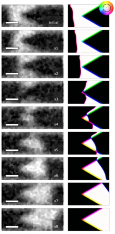
The scanning transmission X-ray microscope at the PolLux endstation was employed to image the operation of a domain-wall NOT gate, allowing the researchers to directly visualize the physical processes driving its operation.
Contacts:
Dr. Jörg Raabe
Swiss Light Source
Paul Scherrer Institut
Telephone: +41 56 310 5193
E-mail: joerg.raabe@psi.ch
Dr. Zhaochu Luo
Paul Scherrer Institut/ETH Zürich
Telephone: +41 56 310 5494
E-mail: zhaochu.luo@psi.ch
Original Publication:
Current-driven magnetic domain-wall logic
Zhaochu Luo, Ales Hrabec, Trong Phuong Dao, Giacomo Sala, Simone Finizio, Junxiao Feng, Sina Mayr, Jörg Raabe, Pietro Gambardella, and Laura J. Heyderman
Nature 579, 214 (2020)
DOI: 10.1038/s41586-020-2061-y
