Show filters
Aus dem Innern einer Eierschale
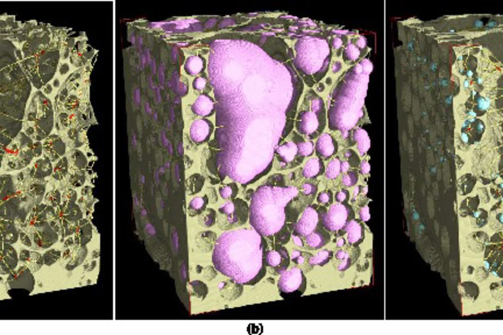
Winzige Bläschen im Innern von Eierschalen liefern die Stoffe, die das Wachstum der Schale stimulieren und steuern. Mit einer neuartigen Tomografie-Technik haben Forschende des Paul Scherrer Instituts PSI, der ETH Zürich und des niederländischen AMOLF-Instituts diese Bläschen erstmals in 3D abbilden können. Sie heben damit eine alte Einschränkung tomografischer Bilder auf und hoffen, dass eines Tages auch die Medizin von ihrer Methode profitiert.
Forschen Richtung Zukunft
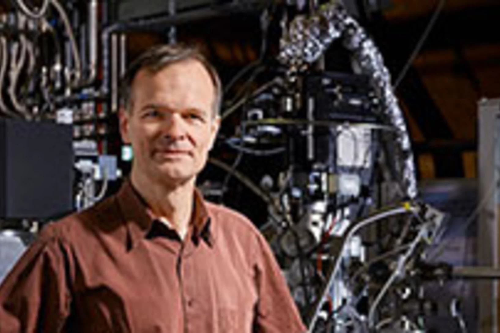
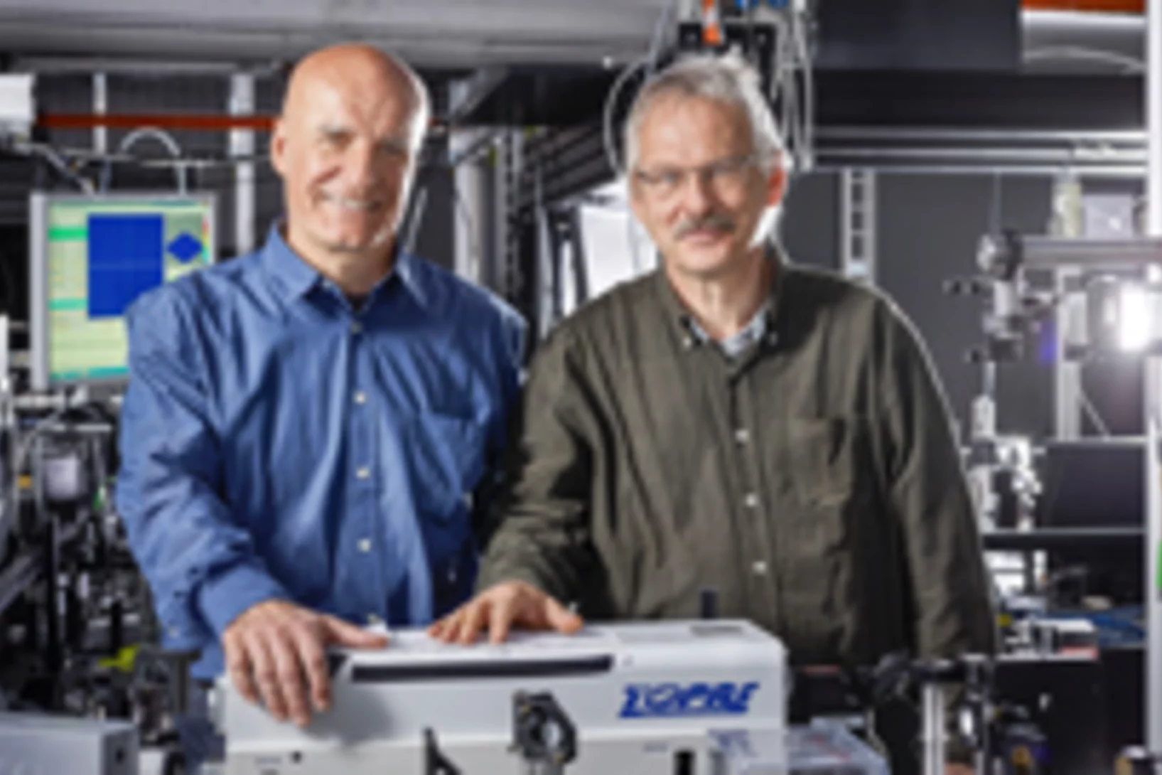
Interview mit Gabriel AeppliSeit 2014 ist Gabriel Aeppli Leiter des Forschungsbereichs Synchrotronstrahlung und Nanotechnologie am PSI. Zuvor hat der gebürtige Schweizer in London ein führendes Forschungszentrum für Nanotechnologie aufgebaut. Im Interview erläutert Aeppli wie sich die Forschungsansätze der Zukunft an den Grossforschungsanlagen des PSI umsetzen lassen und spricht über seinen Blick auf die Schweiz.
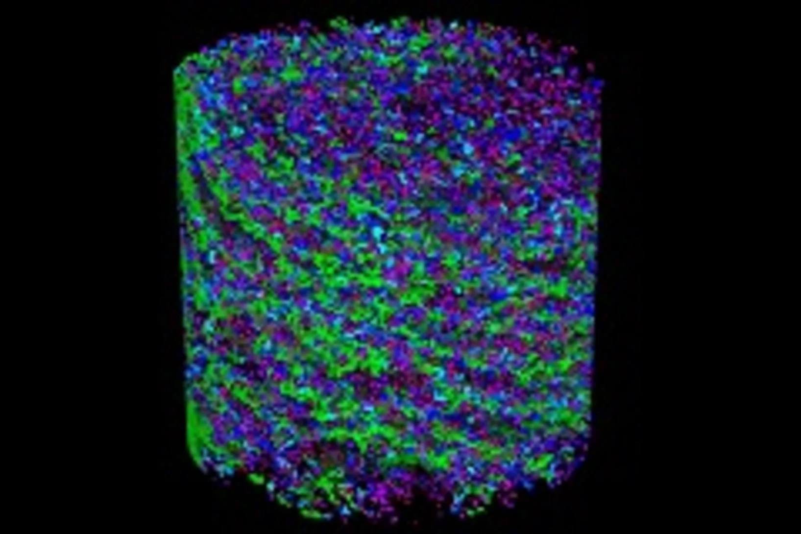
Multiresolution X-ray tomography, getting a clear view of the interior
Researchers at PSI have developed a technique that combines tomography measurements at different resolution levels to allow quantitative interpretation for nanoscale tomography on an interior region of interest of the sample. In collaboration with researchers of the institute AMOLF in the Netherlands and ETH Zurich in Switzerland they showcase their technique by studying the porous structure within a section of an avian eggshell. The detailed measurements of the interior of the sample allowed the researchers to quantify the ordering and distribution of an intricate network of pores within the shell.
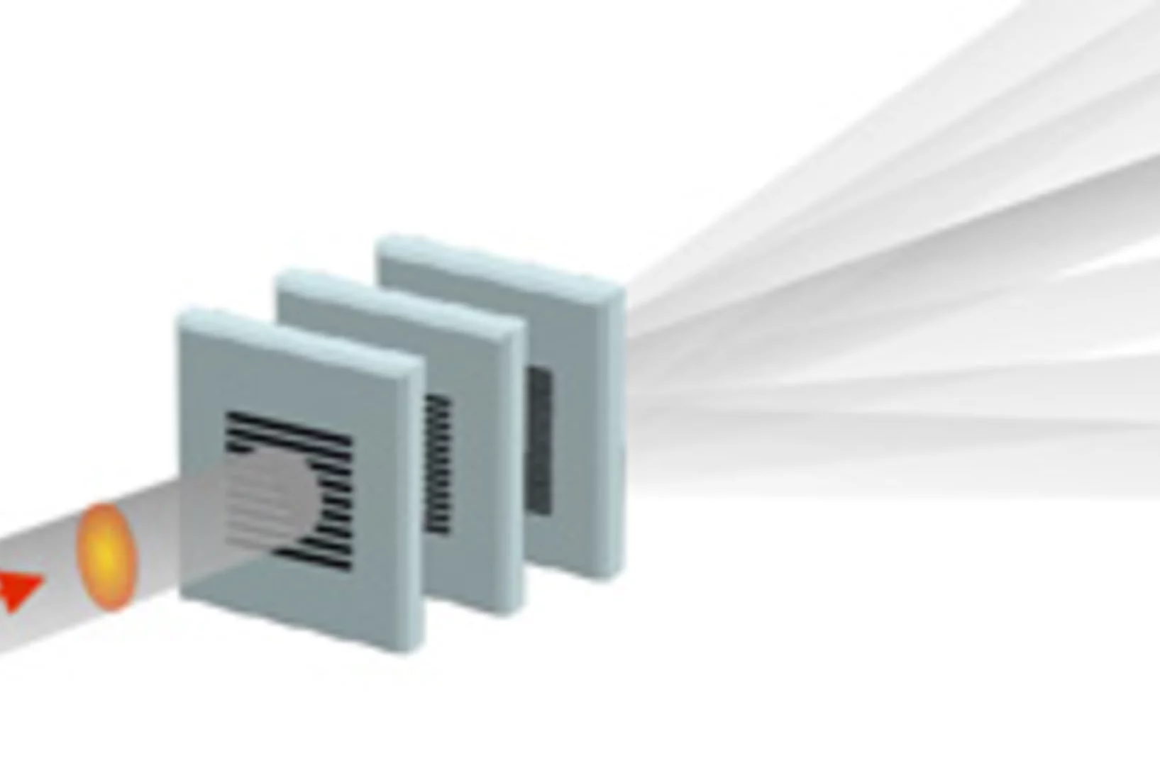
Gespaltener Röntgenblitz zeigt schnelle Vorgänge
SwissFEL, der Röntgenlaser des PSI, wird die einzelnen Schritte sehr schneller Vorgänge sichtbar machen. Ein neues Verfahren soll besonders genaue Experimente ermöglichen: Dabei werden die einzelnen Röntgenblitze in mehrere Teile aufgespalten, die nacheinander am Untersuchungsobjekt ankommen. Das Prinzip des Verfahrens erinnert an die Ideen der frühesten Hochgeschwindigkeitsfotografie.
Nanometer in 3-D
Forschende haben 3-D-Bilder winziger Objekte erzeugt und konnten dabei sogar 25 Nanometer grosse Details (1 Nanometer = 1 Millionstel eines Millimeters) sichtbar machen. Dabei haben sie nicht nur die Form der Untersuchungsgegenstände bestimmen können, sondern auch gezeigt, wie ein bestimmtes chemisches Element (Kobalt) darin verteilt ist und ob es in einer chemischen Verbindung oder in Reinform vorliegt.
Vorbereitet für den SwissFEL
Seit Jahren testen PSI-Forschende Experimentiermethoden, die am Röntgenlaser SwissFEL Einblicke in neuartige Materialien für elektronische Geräte ermöglichen werden. Mit einem besonderen Trick bringen sie dafür die Synchrotron Lichtquelle Schweiz SLS des PSI dazu, Licht zu erzeugen, das ähnliche Eigenschaften hat, wie dasjenige des SwissFEL. So konnten die Forschenden zeigen, dass die geplanten Experimente im Grundsatz möglich sind und den Bau des entsprechenden Messplatzes am SwissFEL vorschlagen.
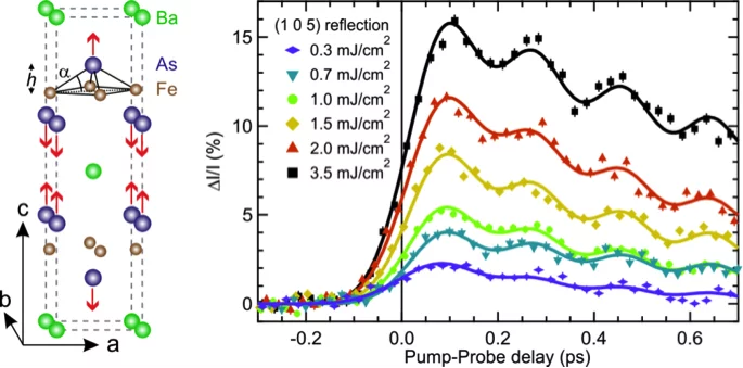
Ultrafast structural dynamics of the Fe-pnictide parent compound BaFe2As2
Understanding the interplay of the various degrees of freedom such as the electrons, spins and lattice is essential for many complex materials, including the high-temperature superconductors.
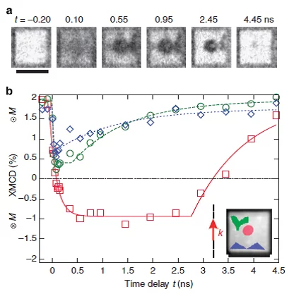
Nanoscale sub-100 picosecond all-optical magnetization switching in GdFeCo microstructure
Ultrafast magnetization reversal driven by femtosecond laser pulses has been shown to be a promising way to write information. Seeking to improve the recording density has raised intriguing fundamental questions about the feasibility of combining ultrafast temporal resolution with sub-wavelength spatial resolution for magnetic recording. Here we report on the experimental demonstration of nanoscale sub-100 ps all-optical magnetization switching, providing a path to sub-wavelength magnetic recording.
Batman zeigt den Weg zu kompakter Datenspeicherung
Forschenden am Paul Scherrer Institut PSI ist es gelungen, winzige magnetische Strukturen mit Laserlicht umzuschalten und die Veränderung zeitlich zu verfolgen. Dabei blinkte kurz ein nanometergrosser Bereich auf, der skurrilerweise an das Fledermaus-Symbol von Batman erinnert. Die Forschungsergebnisse könnten die Datenspeicherung auf Festplatten kompakter, schneller und effizienter machen.
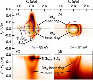
A revealing mixture: The surface of an oxide insulator can host two distinct types of conducting electrons
Strontium titanate, SrTiO3, is an important material for the realization of next-generation electronic devices. A famous example is the interface of LaAlO3 grown on SrTiO3, which is metallic and magnetic at its interface, even though the individual compounds are insulating and nonmagnetic in bulk form. The physics behind how novel interface states form on SrTiO3 - and how they become endowed with such surprising properties - is not well understood.
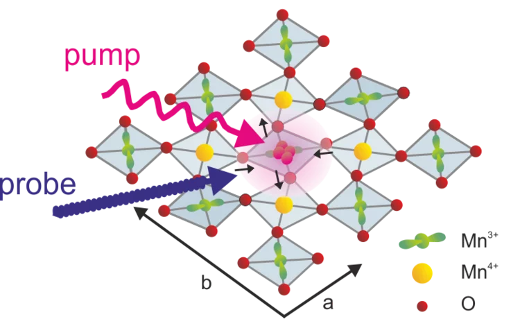
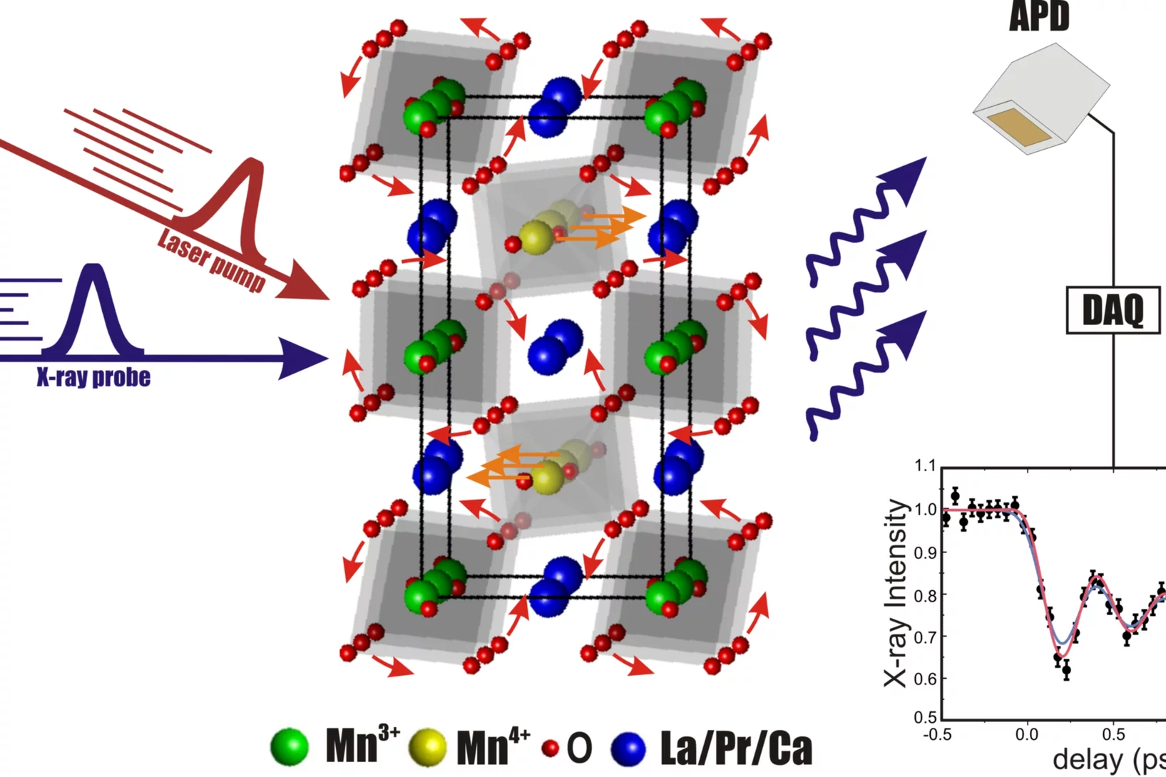
Square dance of the atoms: Shedding light on ultrafast phase transitions
The exploration of the interaction of structural and electronic degrees of freedom in strongly correlated electron systems on the femtosecond time scale is an emerging area of research. One goal of these studies is to advance our understanding of the underlying correlations, another to find ways to control the exciting properties of these materials on an ultrafast time scale.
Observed live with x-ray laser: electricity controls magnetism
Researchers from ETH Zurich and the Paul Scherrer Institute PSI demonstrate how the magnetic structure can be altered quickly in novel materials. The effect could be used in efficient hard drives of the future.
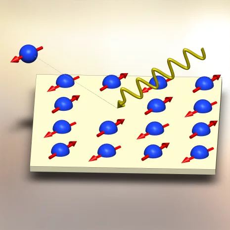
Direct Observation of Magnetic Metastability in Individual Iron Nanoparticles
Studying the magnetization of individual iron (Fe) nanoparticles by magnetic spectromicroscopy reveals that superparamagnetic (SPM) and ferromagnetic blocked (FM) nanoparticles can coexist in the investigated size range of 8-20 nm.
Comprehensive study of the spin-charge interplay in antiferromagnetic La2-xSrxCuO4
The origin of the pseudogap and its relationship with superconductivity in the cuprates remains vague. In particular, the interplay between the pseudogap and magnetism is mysterious. Recent low-temperature angle-resolved photoemission spectroscopy (ARPES) experiments on the underdoped cuprate superconductors indicate the presence of a fully gapped Fermi surface (FS); even in the antiferromagnetic phase.
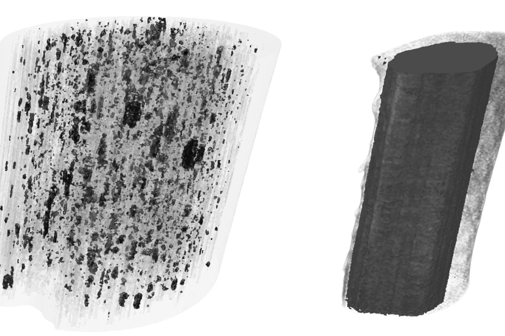
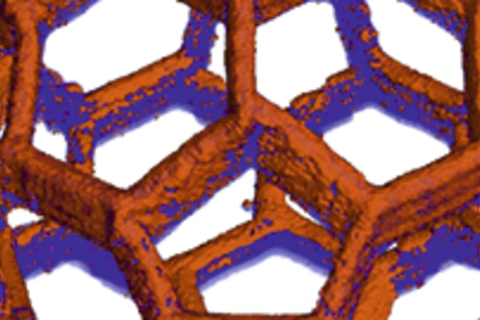
Unique insight into carbon fibers on the nanoscale
Novel carbon materials are promising candidates for light and robust low-cost materials of the future. Understanding their mechanical properties benefits from highly resolved three-dimensional (3D) maps of their porosity and density fluctuations in uninterrupted representative volumes, but these are difficult to obtain with conventional imaging methods.
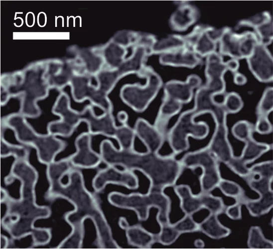
X-ray tomography reaches 16 nm isotropic 3D resolution
Tomographic microscopy has become an invaluable imaging method in both life and materials sciences. Oftentimes, high resolving power is required simultaneously with the ability to characterize large, statistically representative sample volumes. To this task, researchers at the Paul Scherrer Institut have established ptychographic computed tomography.
Spintronics: deciphering a material for future electronics
Topological insulators are the key to future spintronics technologies. EPFL scientists have unraveled how these strange materials work, overcoming one of the biggest obstacles on the way to next-generation applications.Read the full story

Supervolcano eruptions driven by melt buoyancy in large silicic magma chambers
Super-eruptions that dwarf all historical volcanic episodes in erupted volume and environmental impact are abundant in the geological record. Such eruptions of silica-rich magmas form large calderas. The mechanisms that trigger these supereruptions are elusive because the processes occurring in conventional volcanic systems cannot simply be scaled up to the much larger magma chambers beneath super volcanoes.
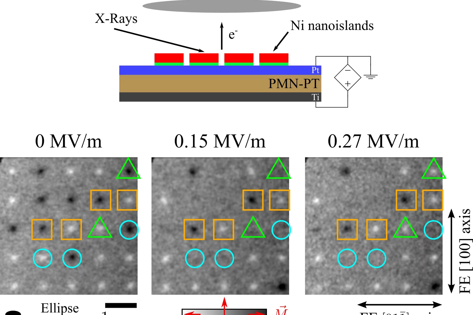
Single Domain Spin Manipulation by Electric Fields in Strain Coupled Artificial Multiferroic Nanostructures
Encoding information by the application of an electric field has a key role in the development of novel memory devices that can operate at high speed while keeping low energy consumption. In magnetoelectric multiferroics, magnetic and ferroelectric ordering coexist and are coupled together so that it is possible to manipulate the material's magnetic structure by applying an electric field with a negligible current flow.

Tiny Magnets as a Model System
Scientists use nano-rods to investigate how matter assembles
In the microscopic world, everything is in motion: atoms and molecules vibrate, proteins fold, even glass is a slow flowing liquid. And during each movement there are interactions between the smallest elements - for example, the atoms - and their neighbours. To make these movements visible, scientists at the Paul Scherrer Institute PSI have developed a special model system.
Atomic motions untangled
The pursuit of capturing motion in a movie bears an obvious fascination irrespective of the time scales involved. In the atomic and molecular world where the masses are so light and the distances small the relevant time scale shifts to the subpicosecond range and the motions become frantic especially for larger molecular systems.
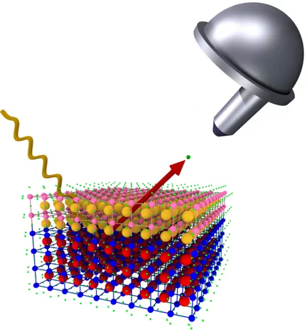
Soft x-ray photoelectron spectroscopy on buried complex oxide interfaces: a new method to diagnose authentic protected electronic structures
Exotic phenomena at interfaces of complex oxides are highly promising for future solid-state electronics applications. A prominent example is the interface of two wide band gap insulators formed by growing a LaAlO3 layer on TiO2-terminated SrTiO3 substrate. When the LaAlO3 thickness exceeds 3 unit cells this system undergoes a sharp insulator-to-metal transition with a two-dimensional electron gas (2DEG) appearing at the interface.
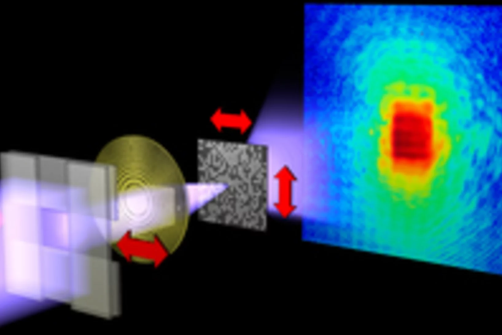
Imaging fluctuations with X-ray microscopy
X-rays allow an inside look at structures that cannot be imaged using visible light. They are used to investigate nanoscale structures of objects as varied as single cells or magnetic storage media. Yet, high-resolution images impose extreme constraints on both the X ray microscope and the samples under investigation.
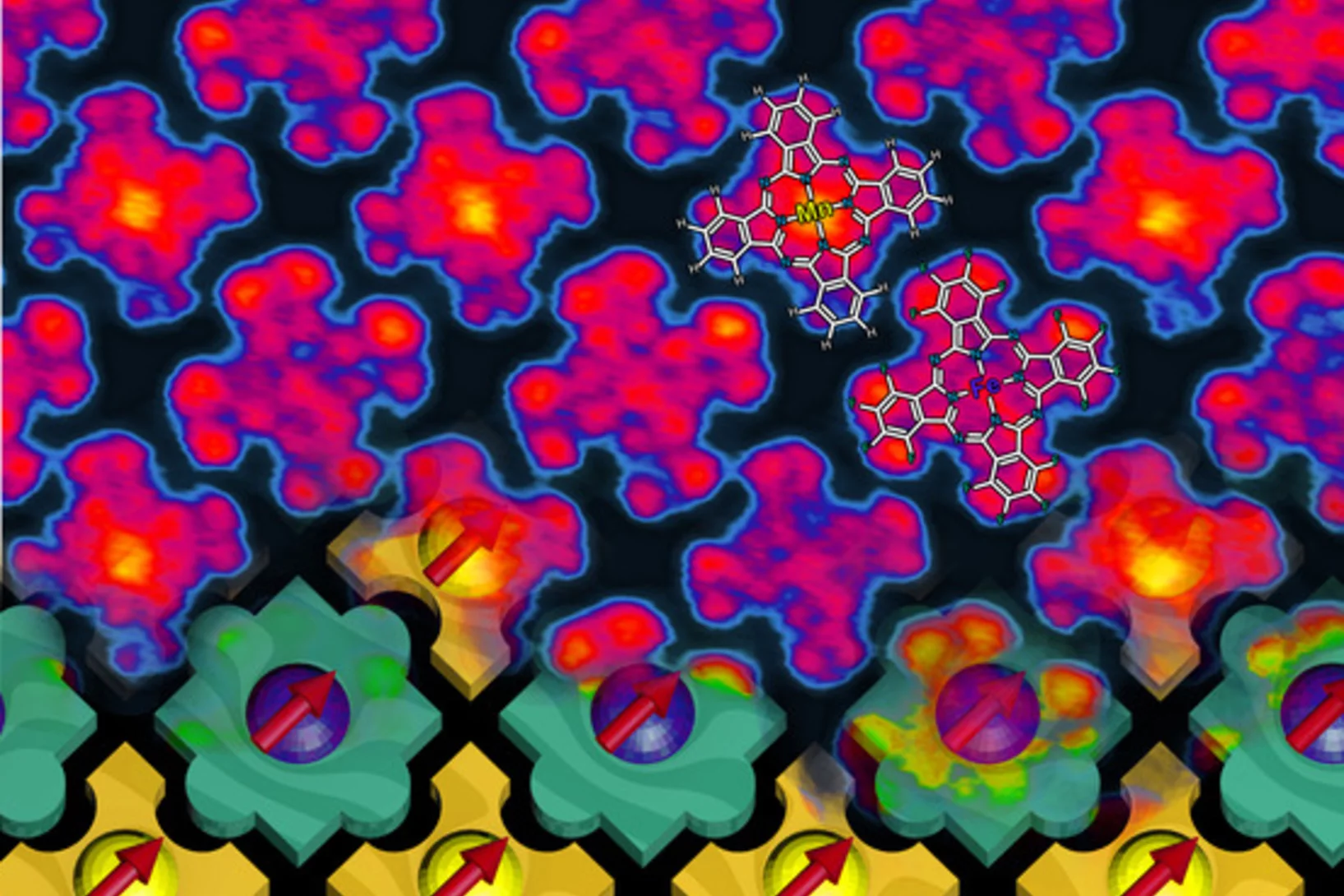
Magnetic nano-chessboard puts itself together
Researchers from the Paul Scherrer Institute and the Indian Institute of Science Education and Research (Pune, India) have managed to ‘turn off’ the magnetization of every second molecule in an array of magnetized molecules and thereby create a ‘magnetic chessboard’. The magnetic molecules were so constructed that they were able to find their places in the nano-chessboard by themselves.
X-rays provide insights into volcanic processes
Experiments performed at the Paul Scherrer Institute (PSI) investigate processes inside volcanic materials that determine whether a volcano will erupt violently or mildly.
New Insights into Superconducting Materials
An American-Swiss research team has used a new X-ray technique at Swiss Light Source (SLS) of the Paul Scherrer Institute (PSI) to investigate the magnetic properties of atomically thin layers of a parent compound of a high-temperature superconductor. It turns out that the magnetic properties of such thin films differ by only a surprisingly small degree from those of macroscopically thick samples.
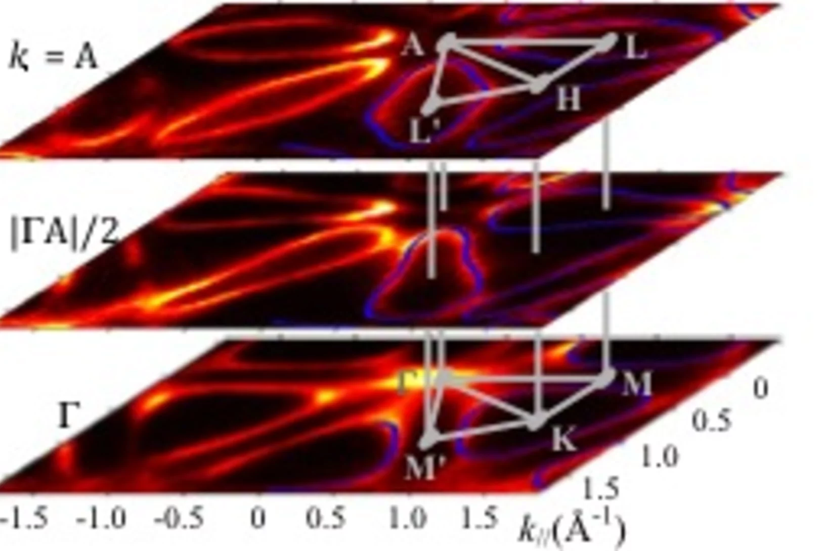
Three-Dimensional Electron Realm in Crystalline Solids Revealed with Soft-X-Rays
The electronic band structure E(k) as energy E of the electrons depending on its wavevector k is the cornerstone concept of the quantum solid state theory. The main experimental method to investigate E(k) is the angle-resolved photoelectron spectroscopy (ARPES). However, a small photoelectron escape depth of a few Å largely restricts the applications of ARPES to two-dimensonal crystals.

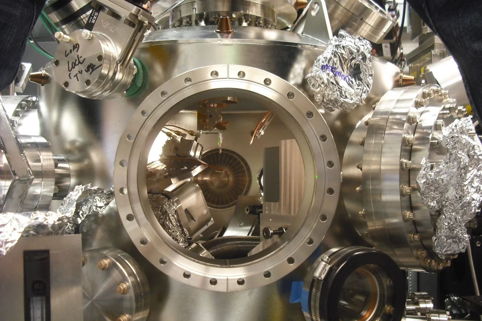
Ultra-short X-ray laser pulses precisely surveyed for the first time
X-ray lasers belong to a modern generation of light sources from which scientists in widely different disciplines expect to obtain new knowledge about the structure and function of materials at the atomic level. On the basis of this new knowledge, it could then be possible one day to develop better medicines, more powerful computers or more efficient catalysts for energy transformation.
Controversy clarified: Why two insulators together can transport electricity
How can two materials which do not conduct electricity create an electrically conducting layer when they are joined together? Since this effect was discovered in 2004, researchers have developed various hypotheses to answer this question – each with its own advocates, who defend it and try to prove its validity. Now, an international team under the leadership of researchers at the Paul Scherrer Institute has probably settled the controversy.
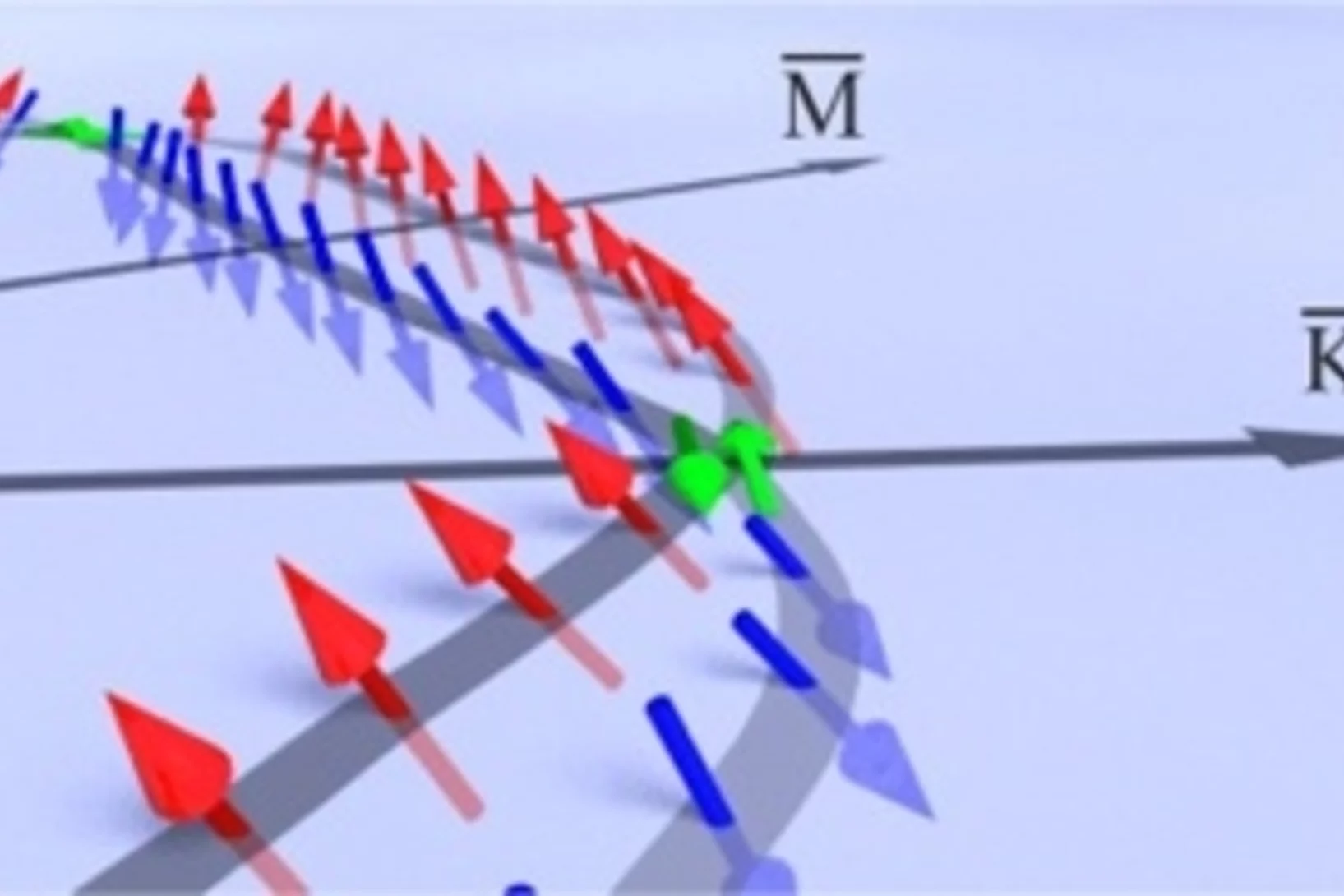
Three-Dimensional Spin Rotations in a Monolayer Electron System
In the emerging field of spintronics, the generation, injection, and in particular the control of highly spin polarized currents are main issues to be solved. Lifting of spin degeneracy by the spin-orbit interaction at surfaces, known as Rashba effect, represents a promising approach, since it generates two spin-polarized bands without the necessity of an external field. In our recent study, we realize such a system for a metallic surface layer on a semiconductor: Au/Ge(111).
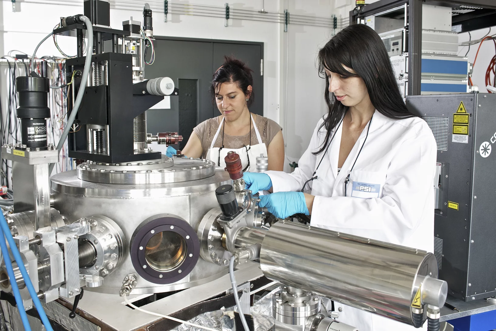
PSI Scientific Reports
Archive 2006-2012. The Scientific Reports – containing accounts of research topics from all the different areas – provide an impression of the variety of subjects researched at PSI.