Thin films are nowadays utilized in many applications, ranging from semiconductor devices to optical coatings and are even present in pharmaceuticals (polymers). This wide-spread application of films with thicknesses from atomic monolayers to microns is due to the developments of thin film deposition techniques. Thin films are also important for studies of materials with new and unique properties due to the possibility of tuning their crystallographic and morphological properties. The thin film approach, i.e. the presence of interfaces (to a substrate or the film surface) adds more degrees of freedom for influencing the properties of materials, e.g. by lattice strain or surface functionalization. For these fundamental studies of material properties large research facilities such as synchrotron radiation or neutron spallation sources are one of the keys that the Paul Scherrer Institute (PSI) provides.
News
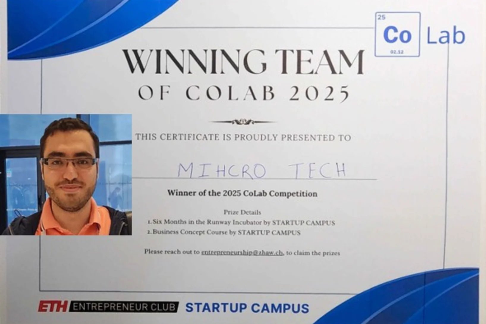
ETH CoLab Award for Mohammadhossein Montazerian
Mohammadhossein Montazerian was part of the winning team to secure an ETH CoLab Award. It is an award to help entrepreneurial research to make a first step towards business.
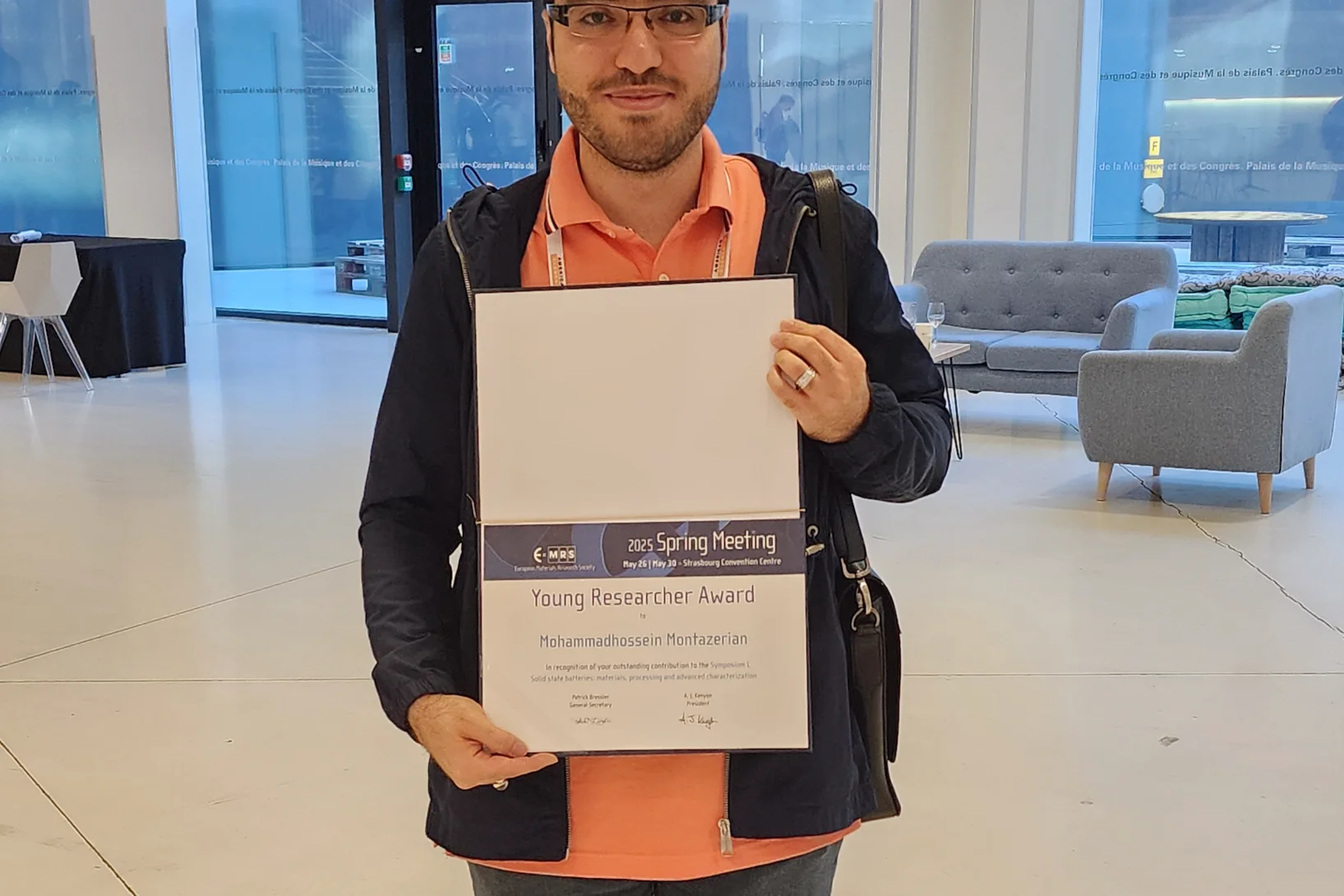
E-MRS 2025 Spring Meeting Young Researcher Award for Mohammadhossein Montazerian
During its recent spring meeting the European Materials Research Society has awarded the E-MRS Young Researcher Award to Mohammadhossein Montazerian from the LMX laboratory in recognition of his "Outstanding contribution to the Symposium L: Solid state batteries - materials, processing and advanced characterization".
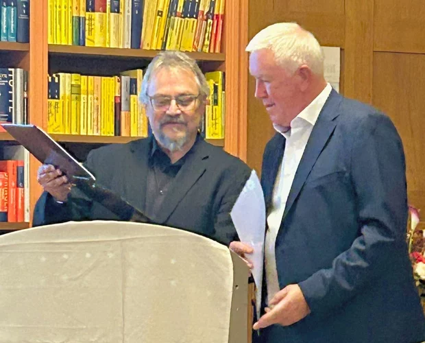
Julius Springer Price 2024
Prof. Thomas Lippert, Editor in Chief at Applied Physics A, awards Prof. Boris Chichkov the 2024 Julius Springer Prize for Applied Physics.
Upcoming Seminars
Upcoming Seminars and Meetings
LMX Meeting: Public PhD Presentation
Date: Thursday 7 May 2026, 13:00
Title: Design and Characterization of Oxynitride Semiconductor Thin Films for Photoelectrocatalytic Water Splitting
Speaker: Kyle Stephens
Room: ODRA/111
CNM Colloquium – Tenure Track Talk
Date: Friday 8. May 2026, 13:00
Title: Designer oxide heterostructures for computing and energy
Speaker: Nikita Shepelin
Room: WLGA/001
TFI Meeting - Canceled due to illness of the speaker
Date: Monday 11 May 2026, 16:00
Title: TBA
Guest Speaker: Dr. Arnold Müller, ETH Zürich, Laboratory of Ion Beam Physics
Room: OFLG/402
TFI Literature Meeting
Date: Monday 18 May 2026, 16:00
Speaker: Kyle Stephens
Room: OFLG/401
TFI Meeting
Date: Tuesday 26 May 2026, 16:00
Title: TBA
Speaker: Pietro Magni
Room: OFLG/402
LMX Meeting
Date: Thursday 28 May 2026, 13:00
Title: Public PhD Presentation
Speaker: Xiaochun Huang
Room: OSGA/EG6b
TFI Literature Meeting
Date: Monday 1 June 2026, 16:00
Speaker: Adil Baiju
Room: OFLG/401
TFI Meeting
Date: Monday 8 June 2026, 16:00
Title: TBA
Guest Speaker: Dr. Morgan Trassin, ETH Zürich, Department of Materials
Room: OFLG/402
Upcoming Conferences
September 2024
iWOE-30 2024
International Workshop on Oxide Electronics
September 29.-2.October 2024 , Darmstadt, Germany
More Information
August 2024
International Mass Spectrometry Conference 2024
Aug. 17-23, 2024
Melbourne, Australia
More Information will be provided here
Scientific Highlights

Characterization of Stable NiOx/ SrTaOxNy Bilayers Boosting the Oxygen Evolution Reaction for Solar Water Splitting
SrTaOxNy (STON) is a well-known visible light-responsive semiconductor with ideally located band edges that allow the operability of overall water splitting. Like many oxynitrides, STON shows evidence of detrimental physicochemical changes under oxygen evolution reaction (OER) conditions involving strong caustic electrolytes. ...

Oxygen-isotope effect on the density wave transitions in La3Ni2O7
The isotope effect is a powerful probe of electron-phonon interactions in solid-state systems, offering key insights into how atomic mass influences emergent quantum states. Here, the impact of oxygen-isotope substitution (16O→18O) on charge- and spin-density wave (CDW and SDW) transitions in the double-layer Ruddlesden-Popper nickelate La3Ni2O7 is investigated ...

Pressure and oxygen-isotope substitution on density-wave transitions in La4Ni3O10
Understanding the interplay between magnetism and superconductivity in nickelate systems is a key objective in condensed matter physics. Gaining microscopic insights into magnetism—particularly as it emerges near superconductivity—requires a synergistic approach that combines complementary experimental techniques with controlled tuning of external parameters. In this paper, we present ...