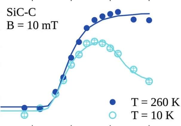
Muon spin rotation with low-energy muons (LE-μSR) is a powerful nuclear method where electrical and magnetic properties of surface-near regions and thin films can be studied on a length scale of ≈200 nm. This study shows the potential of utilizing low-energy muons for a depth-resolved characterization of oxide-semiconductor interfaces, i.e., for silicon (Si) and silicon carbide (4H-SiC). The performance of semiconductor devices relies heavily on the quality of the oxide-semiconductor interface; thus, investigation of defects present in this region is crucial to improve the technology. Silicon dioxide (SiO2) deposited by plasma-enhanced chemical vapor deposition (PECVD) and grown by thermal oxidation of the SiO2-semiconductor interface are compared with respect to interface and defect formation. The nanometer depth resolution of LE-μSR allows for a clear distinction between the oxide and semiconductor layers, while also quantifying the extension of structural changes caused by the oxidation of both Si and SiC. The results demonstrate that LE-μSR can reveal unprecedented details on the structural and electronic properties of the thermally oxidized SiO2-semiconductor interface.
Facility: SμS
Reference: M. Mendes Martins et al, Advanced Materials Interfaces, 2300209 (2023)
Read full article: here


