Direkt zum Inhalt
  • Paul Scherrer Institut PSI
  • PSI Research, Labs & User Services

Digital User Office

  • Digital User Office
  • DE
  • EN
  • FR
Paul Scherrer Institut (PSI)
Suche
Paul Scherrer Institut (PSI)

Hauptnavigation

  • Research at PSIÖffnen dieses Hauptmenu Punktes
    • Research Initiatives
    • Ethics and Research integrity
    • Scientific Highlights
    • Scientific Events
    • Scientific Career
    • PSI-FELLOW
    • PSI Data Policy
  • Research Divisions and LabsÖffnen dieses Hauptmenu Punktes
    • Overview
    • Research with Neutrons and Muons
    • Photon Science
    • Energy and Environment
    • Nuclear Energy and Safety
    • Biology and Chemistry
    • Scientific Computing, Theory and Data
    • Large Research Facilities
  • Facilities and InstrumentsÖffnen dieses Hauptmenu Punktes
    • Overview
    • Large Research Facilities
    • Facilities
    • PSI Facility Newsletter
  • PSI User ServicesÖffnen dieses Hauptmenu Punktes
    • User Office
    • Methods at the PSI User Facilities
    • Proposals for beam time
    • Proposal Deadlines
    • Data Analysis Service (PSD)
    • EU support programmes
  • New ProjectsÖffnen dieses Hauptmenu Punktes
    • SLS 2.0
    • IMPACT
  • DE
  • EN
  • FR

Digital User Office (mobile)

  • Digital User Office

Sie befinden sich hier:

  1. PSI Home
  2. Labs & User Services
  3. PSD
  4. LXN
  5. Research Groups
  6. Molecular Nanoscience
  7. Molecular Electronics

Sekundäre Navigation

Laboratory for X-ray Nanoscience and Technologies (LXN)

  • About LXN
    • Organisational Structure
  • Open Positions
  • People
  • Research Groups Ausgeklappter Submenü Punkt
    • X-ray Nano-Optics
      • X-ray Optics for Imaging and Spectroscopy
        • Fresnel Zone Plate for X-ray Microscopy
        • Blazed X-ray Optics
        • Zernike X-ray Phase Contrast Microscopy
        • Fresnel Zone Plates for RIXS
        • Refractive Lenses by 2 Photon 3D Lithography
      • Wavefront Metrology and Manipulation
        • Vortex Fresnel Zone Plates
        • Grating-based Wavefront Metrology
      • X-ray Optics for XFELs
        • Diamond Fresnel Zone Plates
        • Beam Splitter Gratings for Spectral Monitoring
        • A Delay Line for Ultrafast Pump-Probe Experiments
        • X-ray Streaking for Ultrafast Processes
    • Molecular Nanoscience Ausgeklappter Submenü Punkt
      • On-surface Chemistry
      • Scanning Probe Transport
      • Spins in Molecular Monolayers
      • SiC: Surfaces and Interfaces
      • Our Research Team
    • Advanced Lithography and Metrology
      • EUV Interference Lithography
      • EUV Lensless Imaging
      • ALM Nanoscience
    • Quantum Photon Science
      • News and highlights
      • People
      • Open positions
      • Current projects
        • Imaging quantum many-body states
        • Nonlinear magnonics
        • Optical devices & methods
        • Rare-earth quantum magnets
        • Rydberg states in Si ∂-layers
        • Strained Ge laser (former research activity of H. Sigg & collaborators)
        • Van der Waals materials & devices
      • Infrastructure
        • Cristallina-Q
        • IR beamline
        • Nano-fabrication
      • Publications
      • QTC@PSI
    • Detectors
      • Projects
        • MYTHEN
        • GOTTHARD
        • EIGER
        • JUNGFRAU
        • MOENCH
        • AGIPD
        • Documentation
        • Software Releases
      • Research
      • Detectors Scientific Highlights
      • Publications
      • Team
  • Facilities and Equipment
    • Surface Science Lab
    • Scanning Electron Microscopy
    • Scanning Probe Microscopy
    • PEARL Beamline
    • XIL Facility at the SLS
    • Cleanroom Labs
  • Scientific Highlights and News
    • Archive
  • Publications
    • Archive

Info message

Dieser Inhalt ist nicht auf Deutsch verfügbar.

Doping in Organic Thin Film Transistors

Organic semiconductors are of interest for organic devices such as OLED, solar cells and organic thin film transistors. For such devices it is important to achieve low contact resistance at the metal-organic semiconductor interface, especially for small channel length, and to control the charge carrier density for improved device performance and to obtain specific functionalities. We address these problems by studying the doping of organic thin film transistors with molecular dopants. Especially we investigate the effect of surface doping with different organic molecules on a pentacene thin film transistor. Our transistors consist of only few (2.5-10 ML) monolayer thick active material and both the deposition as well as the electrical characterisation is done in situ in high vacuum.
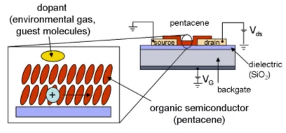
Fig. 1 Scheme of a field effect transistor based on organic molecules
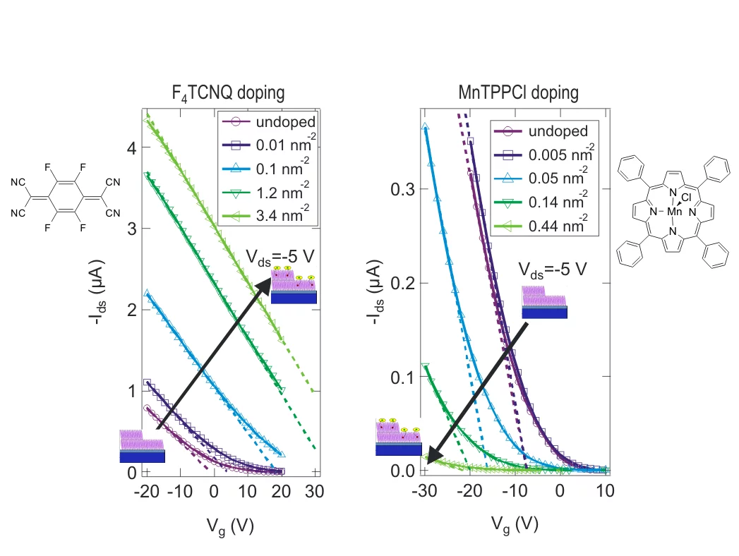
Fig. 2 Shift of transfer curve upon F4TCNQ and MnTPPCl surface doping
We study the doping effects of molecular dopants in organic thin film transistors (TFTs) where we use pentacene as the active organic semiconductor material. Pentacene has a high mobility comparable to the one of amorphous silicon and is a p-type semiconductor. The TFTs consist of a highly doped silicon substrate with a SiO2 layer for the back gate and bottom gold contacts on which the pentacene is evaporated in-situ in high vacuum (Fig. 1).

Doping of such a pentacene TFT can be achieved in two ways: i) by coevaporating pentacene with a small amount of dopant molecules and ii) by surface doping, i.e. by evaporating sub-monolayer films of the dopant molecules on top of the pentacene TFT. In both case we investigate the effect of doping on the transport measurement, e.g. by observing a change of the threshold voltage.

Pentacene doping by coevaporation with the strong acceptor molecule F4TCNQ induces a decrease of the contact resistance by a factor of 20 [1]. Temperature dependent measurements showed that F4TCNQ doping reduces the injection barrier at the pentacene-Au interface and creates acceptor states just below the HOMO level of Pentacene [2].

Surface doping gives us the possibility to gradually increase the doping concentration on one single device and allows easily the study of different dopants. We could achieve both a positive (F4TCNQ) and a negative (MnTPPCl) shift of the threshold voltage (Fig. 2), as well as no change in the transfer characteristics (CoTPP and C60) upon surface doping. [3] By varying the thickness of the pentacene film we could observe a decrease of the maximum threshold shift for channel thickness above 2.5 monolayers of Pentacene. [3]


Publications

1. Reduction of the contact resistance by doping in pentacene few monolayers thin film transistors and self-assembled nanocrystals
C. Vanoni, S. Tsujino and T.A. Jung,
Appl. Phys. Lett. 90, 193119 (2007)

2. Temperature dependent charge-injection at the metal-organic semiconductor interface and density of states in pristine and doped pentacene
C. Vanoni, T.A. Jung, S. Tsujino,
Appl. Phys. Lett. 94, 253306 (2009)

3. Surface doping in pentacene thin-film transistors with few monolayer thick channels
T. Hählen, C. Vanoni, Ch. Wäckerlin, T. A. Jung, and S. Tsujino,
Appl. Phys. Lett. 101, 033305 (2012)

Mit Sidebar

Contact

Prof. Thomas Jung

Laboratory for Molecular Nanoscience
Paul Scherrer Institut
5232 Villigen PSI
Switzerland

Telephone: +41 56 310 45 18
E-mail: thomas.jung@psi.ch

top

Fussbereich

Paul Scherrer Institut

Forschungsstrasse 111
5232 Villigen PSI
Schweiz

Telefon: +41 56 310 21 11
Telefax: +41 56 310 21 99

Der Weg zu uns
Kontakt

Besucherzentrum psi forum
Schülerlabor iLab
Zentrum für Protonentherapie
PSI Bildungszentrum
PSI Guest House (in english)
PSI Gastronomie
psi forum-Shop


Service & Support

  • Telefonbuch
  • User Office
  • Accelerator Status
  • Publikationen des PSI
  • Lieferanten
  • E-Rechnung
  • Computing
  • Sicherheit

Karriere

  • Arbeiten am PSI
  • Stellenangebote
  • Aus- und Weiterbildung
  • Career Center
  • Berufsbildung
  • PSI Bildungszentrum

Für die Medien

  • Das PSI in Kürze
  • Zahlen und Fakten
  • Mediacorner
  • Medienmitteilungen
  • Social Media

Folgen Sie uns: Twitter (deutsch) LinkedIn Youtube Facebook Instagram Issuu RSS

Footer legal

  • Impressum
  • Nutzungsbedingungen
  • Editoren-Login