Direkt zum Inhalt
  • Paul Scherrer Institut PSI
  • PSI Research, Labs & User Services

Digital User Office

  • Digital User Office
  • DE
  • EN
  • FR
Paul Scherrer Institut (PSI)
Suche
Paul Scherrer Institut (PSI)

Hauptnavigation

  • Research at PSIÖffnen dieses Hauptmenu Punktes
    • Research Initiatives
    • Ethics and Research integrity
    • Scientific Highlights
    • Scientific Events
    • Scientific Career
    • PSI-FELLOW
    • PSI Data Policy
  • Research Divisions and LabsÖffnen dieses Hauptmenu Punktes
    • Overview
    • Research with Neutrons and Muons
    • Photon Science
    • Energy and Environment
    • Nuclear Energy and Safety
    • Biology and Chemistry
    • Scientific Computing, Theory and Data
    • Large Research Facilities
  • Facilities and InstrumentsÖffnen dieses Hauptmenu Punktes
    • Overview
    • Large Research Facilities
    • Facilities
    • PSI Facility Newsletter
  • PSI User ServicesÖffnen dieses Hauptmenu Punktes
    • User Office
    • Methods at the PSI User Facilities
    • Proposals for beam time
    • Proposal Deadlines
    • Data Analysis Service (PSD)
    • EU support programmes
  • New ProjectsÖffnen dieses Hauptmenu Punktes
    • SLS 2.0
    • IMPACT
  • DE
  • EN
  • FR

Digital User Office (mobile)

  • Digital User Office

Sie befinden sich hier:

  1. PSI Home
  2. Labs & User Services
  3. PSD
  4. LXN
  5. Research Groups
  6. Advanced Lithography and Metrology
  7. ALM Nanoscience

Sekundäre Navigation

Laboratory for X-ray Nanoscience and Technologies (LXN)

  • About LXN
    • Organisational Structure
  • Open Positions
  • People
  • Research Groups Ausgeklappter Submenü Punkt
    • X-ray Nano-Optics
      • X-ray Optics for Imaging and Spectroscopy
        • Fresnel Zone Plate for X-ray Microscopy
        • Blazed X-ray Optics
        • Zernike X-ray Phase Contrast Microscopy
        • Fresnel Zone Plates for RIXS
        • Refractive Lenses by 2 Photon 3D Lithography
      • Wavefront Metrology and Manipulation
        • Vortex Fresnel Zone Plates
        • Grating-based Wavefront Metrology
      • X-ray Optics for XFELs
        • Diamond Fresnel Zone Plates
        • Beam Splitter Gratings for Spectral Monitoring
        • A Delay Line for Ultrafast Pump-Probe Experiments
        • X-ray Streaking for Ultrafast Processes
    • Molecular Nanoscience
      • On-surface Chemistry
      • Spins in Molecular Monolayers
      • SiC: Surfaces and Interfaces
      • Our Research Team
    • Advanced Lithography and Metrology Ausgeklappter Submenü Punkt
      • EUV Interference Lithography
      • EUV Lensless Imaging
      • ALM Nanoscience
    • Quantum Photon Science
      • News and highlights
      • People
      • Open positions
      • Current projects
        • Imaging quantum many-body states
        • Nonlinear magnonics
        • Optical devices & methods
        • Rare-earth quantum magnets
        • Rydberg states in Si ∂-layers
        • Strained Ge laser (former research activity of H. Sigg & collaborators)
        • Van der Waals materials & devices
      • Infrastructure
        • Cristallina-Q
        • IR beamline
        • Nano-fabrication
      • Publications
      • QTC@PSI
    • Detectors
      • Projects
        • MYTHEN
        • GOTTHARD
        • EIGER
        • JUNGFRAU
        • MOENCH
        • AGIPD
        • Documentation
        • Software Releases
      • Research
      • Detectors Scientific Highlights
      • Publications
      • Team
  • Facilities and Equipment
    • Surface Science Lab
    • Scanning Electron Microscopy
    • Scanning Probe Microscopy
    • PEARL Beamline
    • XIL Facility at the SLS
    • Cleanroom Labs
  • Scientific Highlights and News
    • Archive
  • Publications
    • Archive

Info message

Dieser Inhalt ist nicht auf Deutsch verfügbar.

Nanophotonics

Metallic nanostructures smaller than wavelength of interacting radiation have interesting far-field and near-field optical properties. For instance, the electromagnetic fields near such structures (near fields) are significantly amplified. This phenomenon is important for applications such as near-field microscopy, biosensing, surface enhanced Raman spectroscopy and nano-antennae. Also far-field properties of such structures are substantially different and can be tailored resulting in exciting phenomena such as extraordinary transmission through subwavelength hole arrays, negative refractive index, and strong birefringence. Our aim is to design novel nanomaterials for potential applications in nanophotonics, nanoplasmonics, biosensing and optical devices. The fabrication methods involve e-beam lithography and extreme ultraviolet interference lithography.

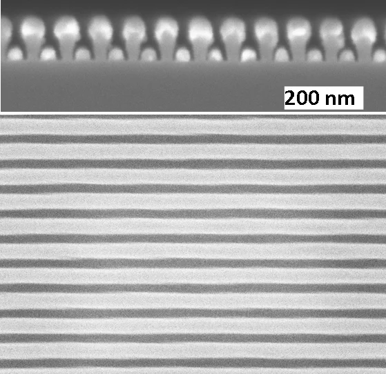
Top-down and cross-sectional SEM images of Al bilayer wire-grid polarizers.
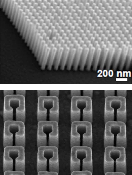
SEM images of high aspect ratio plasmonic nanostructures.
Selected Publications

Distributing the optical near-field for efficient field-enhancements in nanostructures,
V. K. Valev, B. De Clercq, C. G. Biris, X. Zheng, S. Vandendriessche, M. Hojeij, D. Denkova, Y. Jeyaram, N. C. Panoiu, Y. Ekinci, A. V. Silhanek, V. Volskiy, G. A. E. Vandenbosch, M. Ameloot, V. V. Moshchalkov, and T. Verbiest,
Adv. Mater. (2012).

Deep-ultraviolet surface-enhanced resonance Raman scattering of adenine on aluminum nanoparticle arrays,
S. K. Jha, Z. Ahmed, M. Agio, Y. Ekinci, and J. F. Löffler,
J. Am. Chem. Soc. 134, 1966 (2012).

High Aspect Ratio Plasmonic Nanostructures for Sensing Applications,
B. Päivänranta, H. Merbold, R. Giannini, L. Buechi, S. Gorelick, C. David, J. F. Löffler, T. Feurer, Y. Ekinci,
ACS Nano 5, 6374 (2011).

Nanofluidics

Trapping, sorting and manipulation of nanoparticles in solution are of great interest for applications in soft condensed matter, biology, and medicine. We develop methods and devices based on nanofluidics for reliable, high-throughput and contact-free trapping, manipulation of nanoparticles and nano-objects.

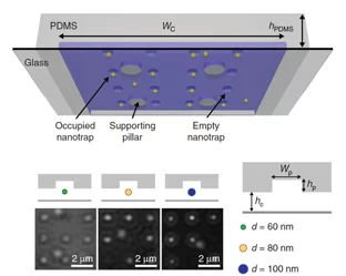
Schematic of the PDMS-based nanofluidic trapping device with integrated pockets and supporting
pillars. The nanofluidic channels had a width of several micrometers and the height is a few hundred nanometers and nanopockets.  Below show the optical images of trapped nanoparticles.
Schematic of the PDMS-based nanofluidic trapping device with integrated pockets and supporting
pillars. The nanofluidic channels had a width of several micrometers and the height is a few hundred nanometers and nanopockets. Below show the optical images of trapped nanoparticles.
Selected Publications

Soft electrostatic trapping in nanofluidics
M. A. Gerspach, N. Mojarad, D. Sharma, T. Pfohl, and Y. Ekinci
Nature Microsystems & Nanoengineering 3, 17051 (2017)

Nanofluidic lab-on-a-chip trapping devices for screening electrostatics in concentration gradients
M. A. Gerspach, N. Mojarad, D. Sharma, T. Pfohl, and Y. Ekinci
Microelectronic Eng. 175, 17 (2017)

Nanowires

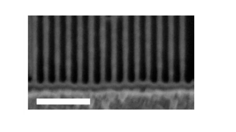
Suspended silicon nanowires fabricated using EUV interference lithography.
Selected Publications

Strain and thermal conductivity in ultra-thin suspended silicon nanowires
D. Fan, H. Sigg, R. Spolenak, and Y. Ekinci
Physical Review B 96, 115307 (2017)

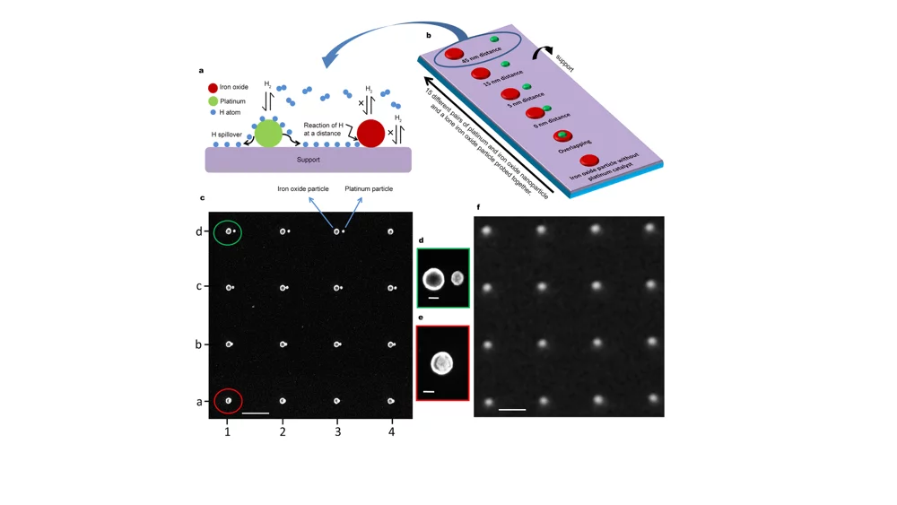
Nanocatalysis

Schematic  mechanism of hydrogen spillover. Iron and platinum nanoparticules with  variable distance. SEM and PEEM images of the nanoparticle pairs.
Schematic mechanism of hydrogen spillover. Iron and platinum nanoparticules with variable distance. SEM and PEEM images of the nanoparticle pairs.
Selected Publications

Catalyst support effects on hydrogen spillover
W. Karim, C. Spreafico, A. Kleibert, J. Gobrecht, J. VandeVondele, Y. Ekinci, and J. A. van Bokhoven
Nature 541, 68 (2017)

Size-dependent redox behavior of iron observed by in-situ single nanoparticle spectro-microscopy on well-defined model systems
W. Karim, A. Kleibert, U. Hartfelder, A. Balan, J. Gobrecht, J. A. van Bokhoven, and Y. Ekinci
Scientific Reports 6, 18818 (2016)


Mit Sidebar

Contact

Dr. Yasin Ekinci

Laboratory for X-ray Nanoscience and
Technologies

Paul Scherrer Institut
5232 Villigen PSI
Switzerland

Telephone: +41 56 310 28 24
E-mail: yasin.ekinci@psi.ch

top

Fussbereich

Paul Scherrer Institut

Forschungsstrasse 111
5232 Villigen PSI
Schweiz

Telefon: +41 56 310 21 11
Telefax: +41 56 310 21 99

Der Weg zu uns
Kontakt

Besucherzentrum psi forum
Schülerlabor iLab
Zentrum für Protonentherapie
PSI Bildungszentrum
PSI Guest House (in english)
PSI Gastronomie
psi forum-Shop


Service & Support

  • Telefonbuch
  • User Office
  • Accelerator Status
  • Publikationen des PSI
  • Lieferanten
  • E-Rechnung
  • Computing
  • Sicherheit

Karriere

  • Arbeiten am PSI
  • Stellenangebote
  • Aus- und Weiterbildung
  • Career Center
  • Berufsbildung
  • PSI Bildungszentrum

Für die Medien

  • Das PSI in Kürze
  • Zahlen und Fakten
  • Mediacorner
  • Medienmitteilungen
  • Social Media

Folgen Sie uns: Twitter (deutsch) LinkedIn Youtube Facebook Instagram Issuu RSS

Footer legal

  • Impressum
  • Nutzungsbedingungen
  • Editoren-Login