The digital world surrounding us is based on Si CMOS technology. The constant improvement of the transistor performances observed in the last fifty years is nevertheless approaching an end, encouraging the development of new concepts to supply the continuously increasing demand for information technologies. Si photonics, one of the most promising concepts, envisages the integration of photonics into the current electrical platforms. Although integration of some photonic elements – such as modulators, splitters etc. – is possible on a large scale, unfortunately Si, by fundamental reasons, lacks to be an efficient light emitter. A visionary way out of this dilemma is to use Ge instead of silicon, which, thanks to its CMOS compatibility and favourable bandstructure under tensile strain and/or when alloyed with Sn, could make up for this particular shortcoming of Si.
Here, at PSI, we followed these two major concepts:
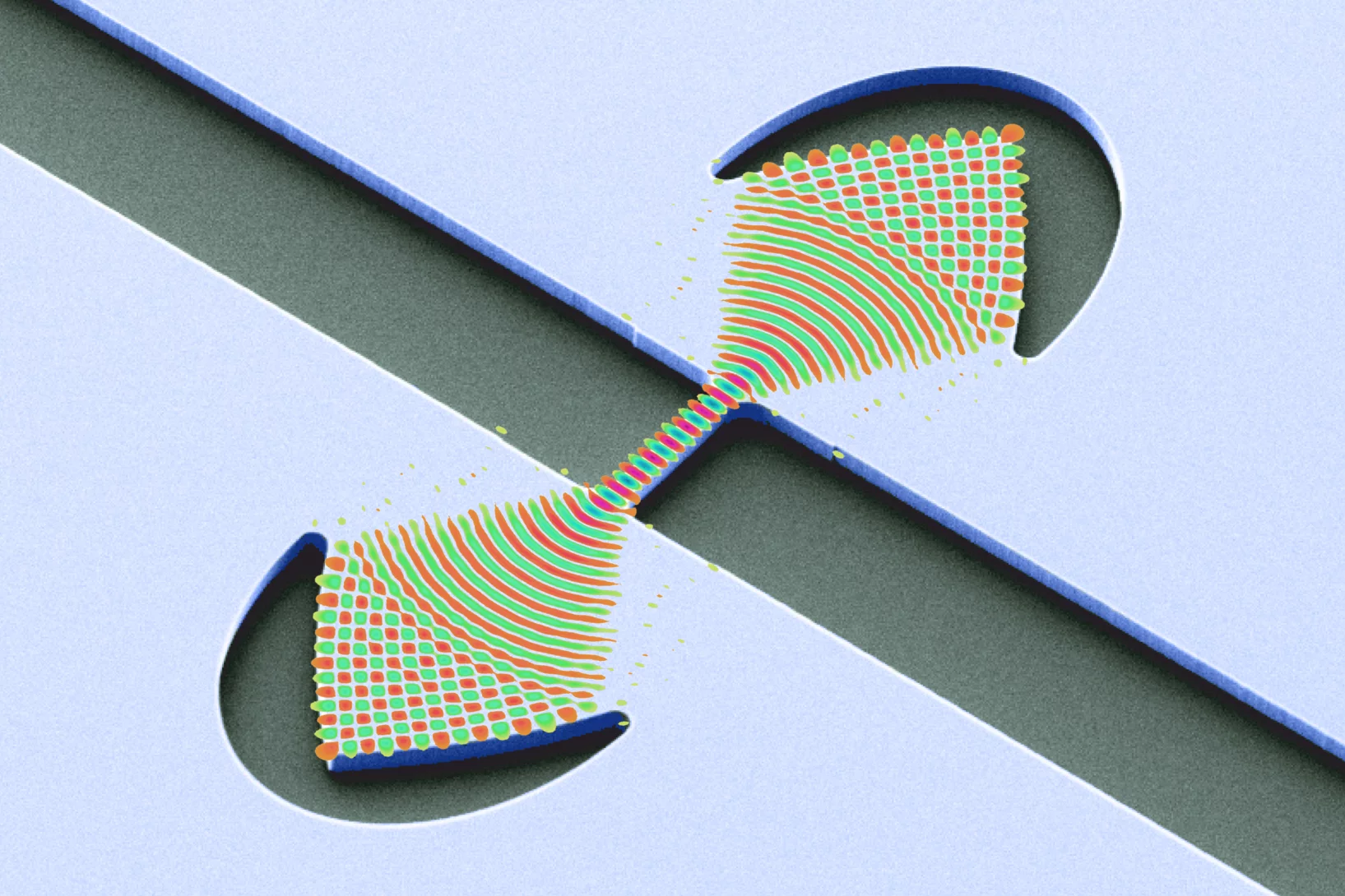
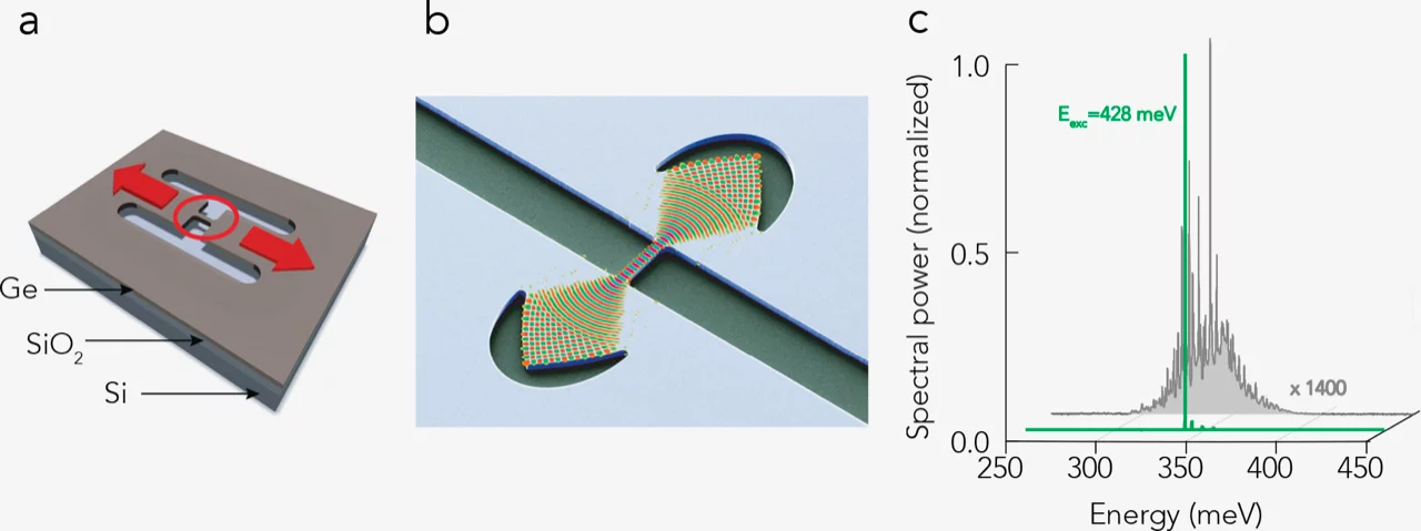
(a) Based on the here developed strain amplification concept, in collaboration with CEA Grenoble and ETH Zürich, we have demonstrated the first interband laser from elemental Ge. When the Ge microbridges are loaded up to 6% of strain, and integrated into an optical cavity highly efficient lasing is observed up to temperatures of 100 K.
(b) Alternatively, GeSn alloys with ~8% Sn concentration or more become a direct bandgap semiconductor, which is the basic requirement for a material to be able to lase. Our collaboration with the Forschungszentrum Jülich and CEA Grenoble was the first to demonstrate this effect. Lasing in these alloys represents the first step towards a purely group IV epitaxially defined laser that can be produced with similar fabrication methods as state-of-the-art III-V semiconductor lasers.

Recent publications
Investigation of lasing in highly strained germanium at the crossover to direct band gap
F. T. Armand Pilon, Y-M. Niquet, J. Chretien, N. Pauc, V. Reboud, V. Calvo, J. Widiez , J. M. Hartmann, A. Chelnokov, J. Faist, H. Sigg
Phys. Rev. Research 4, 033050 (2022)
Lasing in strained germanium microbridges
F. T. Armand Pilon, A. Lyasota, Y.-M. Niquet, V. Reboud, V. Calvo, N. Pauc, J. Widiez, C. Bonzon, J. M. Hartmann, A. Chelnokov, J. Faist, H. Sigg
Nat. Commun. 10, 2724 (2019)
Top-down method to introduce ultra-high elastic strain
T. Zabel, R. Geiger, E. Marin, E. Müller, A. Diaz, C. Bonzon, M. J. Süess, R. Spolenak, J. Faist, H. Sigg
J. Mater. Res. 32, 726 (2017)
Optically pumped GeSn micro-disks with 16% Sn lasing at 3.1 μm up to 180 K
V. Reboud, A. Gassenq, N. Pauc, J. Aubin, L. Milord, Q. M. Thai, M. Bertrand, K. Guilloy, D. Rouchon, J. Rothman, T. Zabel, F. Armand Pilon, H. Sigg, A. Chelnokov, J. M. Hartmann, V. Calvo
Appl. Phys. Lett. 111, 092101 (2017)
Optically pumped GeSn microdisk lasers on Si
D. Stange, S. Wirths, R. Geiger, C. Schulte-Braucks, B. Marzban, N. von den Driesch, G. Mussler, T. Zabel, T. Stoica, J.-M. Hartmann, S. Mantl, Z. Ikonic, D. Grützmacher, H. Sigg, J. Witzens, D. Buca
ACS Photonics 3, 1279 (2016)
Lasing in direct-bandgap GeSn alloy grown on Si
S. Wirths, R. Geiger, N. von den Driesch, G. Mussler, T. Stoica, S. Mantl, Z. Ikonic, M. Luysberg, S. Chiussi, J. M. Hartmann, H. Sigg, J. Faist, D. Buca, D. Grützmacher
Nat. Photon. 9, 88 (2015).
Analysis of enhanced light emission from highly strained germanium microbridges
M. J. Süess, R. Geiger, R. A. Minamisawa, G. Schiefler, J. Frigeri, D. Chrastina, G. Isella, R. Spolenak, J. Faist, H. Sigg
Nat. Photon. 7, 466 (2013)