Aller au contenu principal
  • Paul Scherrer Institut PSI
  • PSI Research, Labs & User Services

Digital User Office

  • Digital User Office
  • DE
  • EN
  • FR
Paul Scherrer Institut (PSI)
Rechercher
Paul Scherrer Institut (PSI)

Hauptnavigation

  • Research at PSIOuvrir ce point de menu principal
    • Research Initiatives
    • Ethics and Research integrity
    • Scientific Highlights
    • Scientific Events
    • Scientific Career
    • PSI-FELLOW
    • PSI Data Policy
  • Research Divisions and LabsOuvrir ce point de menu principal
    • Overview
    • Research with Neutrons and Muons
    • Photon Science
    • Energy and Environment
    • Nuclear Energy and Safety
    • Biology and Chemistry
    • Scientific Computing, Theory and Data
    • Large Research Facilities
  • Facilities and InstrumentsOuvrir ce point de menu principal
    • Overview
    • Large Research Facilities
    • Facilities
    • PSI Facility Newsletter
  • PSI User ServicesOuvrir ce point de menu principal
    • User Office
    • Methods at the PSI User Facilities
    • Proposals for beam time
    • Proposal Deadlines
    • Data Analysis Service (PSD)
    • EU support programmes
  • New ProjectsOuvrir ce point de menu principal
    • SLS 2.0
    • IMPACT
  • DE
  • EN
  • FR

Digital User Office (mobile)

  • Digital User Office

Vous êtes ici:

  1. PSI Home
  2. Labs & User Services
  3. PSD
  4. LXN
  5. Research Groups
  6. Quantum Photon Science
  7. Current projects
  8. Strained Ge laser (former research activity of H. Sigg & collaborators)

Navigation secondaire

Laboratory for X-ray Nanoscience and Technologies (LXN)

  • About LXN
    • Organisational Structure
  • Open Positions
  • People
  • Research Groups Sous-menu élargi
    • X-ray Nano-Optics
      • X-ray Optics for Imaging and Spectroscopy
        • Fresnel Zone Plate for X-ray Microscopy
        • Blazed X-ray Optics
        • Zernike X-ray Phase Contrast Microscopy
        • Fresnel Zone Plates for RIXS
        • Refractive Lenses by 2 Photon 3D Lithography
      • Wavefront Metrology and Manipulation
        • Vortex Fresnel Zone Plates
        • Grating-based Wavefront Metrology
      • X-ray Optics for XFELs
        • Diamond Fresnel Zone Plates
        • Beam Splitter Gratings for Spectral Monitoring
        • A Delay Line for Ultrafast Pump-Probe Experiments
        • X-ray Streaking for Ultrafast Processes
    • Molecular Nanoscience
      • On-surface Chemistry
      • Spins in Molecular Monolayers
      • SiC: Surfaces and Interfaces
      • Our Research Team
    • Advanced Lithography and Metrology
      • EUV Interference Lithography
      • EUV Lensless Imaging
      • ALM Nanoscience
    • Quantum Photon Science Sous-menu élargi
      • News and highlights
      • People
      • Open positions
      • Current projects Sous-menu élargi
        • Imaging quantum many-body states
        • Nonlinear magnonics
        • Optical devices & methods
        • Rare-earth quantum magnets
        • Rydberg states in Si ∂-layers
        • Strained Ge laser (former research activity of H. Sigg & collaborators)
        • Van der Waals materials & devices
      • Infrastructure
        • Cristallina-Q
        • IR beamline
        • Nano-fabrication
      • Publications
      • QTC@PSI
    • Detectors
      • Projects
        • MYTHEN
        • GOTTHARD
        • EIGER
        • JUNGFRAU
        • MOENCH
        • AGIPD
        • Documentation
        • Software Releases
      • Research
      • Detectors Scientific Highlights
      • Publications
      • Team
  • Facilities and Equipment
    • Surface Science Lab
    • Scanning Electron Microscopy
    • Scanning Probe Microscopy
    • PEARL Beamline
    • XIL Facility at the SLS
    • Cleanroom Labs
  • Scientific Highlights and News
    • Archive
  • Publications
    • Archive

Info message

Ce contenu n'est pas disponible en français.

Strained Ge laser (former research activity of H. Sigg & collaborators)

The digital world surrounding us is based on Si CMOS technology. The constant improvement of the transistor performances observed in the last fifty years is nevertheless approaching an end, encouraging the development of new concepts to supply the continuously increasing demand for information technologies. Si photonics, one of the most promising concepts, envisages the integration of photonics into the current electrical platforms. Although integration of some photonic elements – such as modulators, splitters etc. – is possible on a large scale, unfortunately Si, by fundamental reasons, lacks to be an efficient light emitter. A visionary way out of this dilemma is to use Ge instead of silicon, which, thanks to its CMOS compatibility and favourable bandstructure under tensile strain and/or when alloyed with Sn, could make up for this particular shortcoming of Si.

Here, at PSI, we followed these two major concepts:

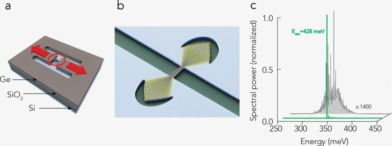
(a) Based on the here developed strain amplification concept, in collaboration with CEA Grenoble and ETH Zürich, we have demonstrated the first interband laser from elemental Ge. When the Ge microbridges are loaded up to 6% of strain, and integrated into an optical cavity highly efficient lasing is observed up to temperatures of 100 K.

ge_laser1
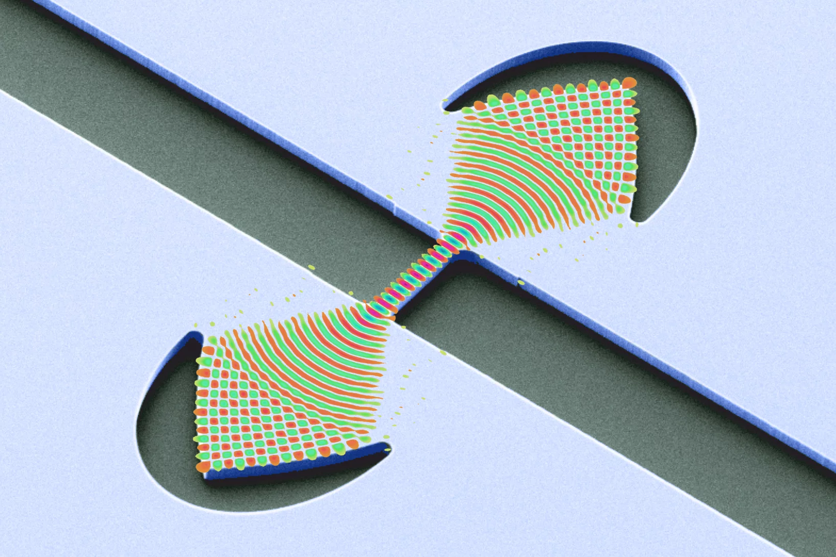
Figure 1 | (a) Illustration of the strain enhancement process: once the underlying SiO2 is removed, the pads relax and thus stretch the microbridge. (b) Scanning electron microscopy view of a strained microbridge integrated into a corner cube cavity; superimposed is the simulated high quality-factor cavity mode. (c) Below and above threshold emission spectra showing striking contrast between multi-line (grey) and orders of magnitude more intense lasing emission (green).

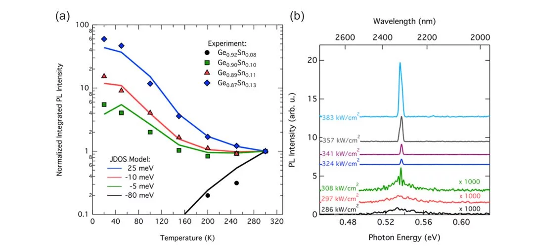
(b) Alternatively, GeSn alloys with ~8% Sn concentration or more become a direct bandgap semiconductor, which is the basic requirement for a material to be able to lase. Our collaboration with the Forschungszentrum Jülich and CEA Grenoble was the first to demonstrate this effect. Lasing in these alloys represents the first step towards a purely group IV epitaxially defined laser that can be produced with similar fabrication methods as state-of-the-art III-V semiconductor lasers.

Figure 3 (a) Integrated photoluminescence intensity from various GeSn alloys. Coloured curves show the modeled intensity obtained from joint density of states calculations with the band offset ΔE between Γ and L valley. (b) Excitation power dependent photoluminescence showing
Figure 2 | (a) Integrated photoluminescence intensity from various GeSn alloys. Lines represent the modelled intensity obtained from joint density of states calculations with a band offset ΔE between the Γ and L valley. (b) Excitation power dependent photoluminescence.

Recent publications

Investigation of lasing in highly strained germanium at the crossover to direct band gap
F. T. Armand Pilon, Y-M. Niquet, J. Chretien, N. Pauc, V. Reboud, V. Calvo, J. Widiez , J. M. Hartmann, A. Chelnokov, J. Faist, H. Sigg
Phys. Rev. Research 4, 033050 (2022)

Lasing in strained germanium microbridges
F. T. Armand Pilon, A. Lyasota, Y.-M. Niquet, V. Reboud, V. Calvo, N. Pauc, J. Widiez, C. Bonzon, J. M. Hartmann, A. Chelnokov, J. Faist, H. Sigg
Nat. Commun. 10, 2724 (2019)

Top-down method to introduce ultra-high elastic strain
T. Zabel, R. Geiger, E. Marin, E. Müller, A. Diaz, C. Bonzon, M. J. Süess, R. Spolenak, J. Faist, H. Sigg
J. Mater. Res. 32, 726 (2017)

Optically pumped GeSn micro-disks with 16% Sn lasing at 3.1 μm up to 180 K
V. Reboud, A. Gassenq, N. Pauc, J. Aubin, L. Milord, Q. M. Thai, M. Bertrand, K. Guilloy, D. Rouchon, J. Rothman, T. Zabel, F. Armand Pilon, H. Sigg, A. Chelnokov, J. M. Hartmann, V. Calvo
Appl. Phys. Lett. 111, 092101 (2017)

Optically pumped GeSn microdisk lasers on Si
D. Stange, S. Wirths, R. Geiger, C. Schulte-Braucks, B. Marzban, N. von den Driesch, G. Mussler, T. Zabel, T. Stoica, J.-M. Hartmann, S. Mantl, Z. Ikonic, D. Grützmacher, H. Sigg, J. Witzens, D. Buca
ACS Photonics 3, 1279 (2016)

Lasing in direct-bandgap GeSn alloy grown on Si
S. Wirths, R. Geiger, N. von den Driesch, G. Mussler, T. Stoica, S. Mantl, Z. Ikonic, M. Luysberg, S. Chiussi, J. M. Hartmann, H. Sigg, J. Faist, D. Buca, D. Grützmacher
Nat. Photon. 9, 88 (2015).

Analysis of enhanced light emission from highly strained germanium microbridges
M. J. Süess, R. Geiger, R. A. Minamisawa, G. Schiefler, J. Frigeri, D. Chrastina, G. Isella, R. Spolenak, J. Faist, H. Sigg
Nat. Photon. 7, 466 (2013)


Recent highlights

1 juillet 2019
LaserImage

First demonstration of a Germanium laser

Scientist at the Paul Scherrer Institut and ETH Zürich, with colleagues from CEA Grenoble, have demonstrated and characterized a technology that, for the first time, yields lasing from strained elemental Germanium. This achievement underlines PSI’s leading role in the development of Silicon-compatible laser light sources.

En savoir plus

Project members

Photo of Stefan Stutz
Stefan Stutz

Spektroskopie Techniker

+41 56 310 45 65
stefan.stutz@psi.ch
Hans Sigg
Dr. Hans-Christian Sigg

Scientific Advisor  Quantum Technologies

+41 56 310 40 48
hans.sigg@psi.ch

Sidebar

Contact

Dr. Simon Gerber

Laboratory for X-ray Nanoscience and Technologies
Paul Scherrer Institut
5232 Villigen PSI
Switzerland

Telephone: +41 56 310 39 65
E-mail: simon.gerber@psi.ch
top

Pied de page

Paul Scherrer Institut

Forschungsstrasse 111
5232 Villigen PSI
Suisse

Téléphone: +41 56 310 21 11
Téléfax: +41 56 310 21 99

Comment nous trouver 
Contact

Centre de visiteurs psi forum
Laboratoire élèves iLab (en allemand)
Centre de protonthérapie
Centre de Formation du PSI (en allemand)
PSI Guest House (en anglais)
PSI Gastronomie (en allemand)
psi forum shop

Service & Support

  • Annuaire
  • User Office
  • Accelerator Status
  • Publications du PSI
  • Fournisseurs
  • E-facture
  • Computing (en anglais)
  • Sicherheit (en allemand)

Carrière

  • Travailler au PSI
  • Offres d'emploi
  • Formation initiale et formation continue
  • Career Center
  • Formation professionnelle (en allemand)
  • Centre de Formation du PSI

Pour les médias

  • Le PSI en bref
  • Chiffres et faits
  • Le coin médias
  • Communiqués de presse
  • Réseaux sociaux

Suivez le PSI: Twitter (in English) LinkedIn Youtube Facebook Instagram Issuu RSS

Footer legal

  • Impressum
  • Conditions d'utilisation
  • Login éditeurs