

Since a long time, experts have been trying to find a way to realize a laser for monolithic integration into Silicon-based chip technology, which would drastically improve the performances of processors. Now, scientist at the Paul Scherrer Institut and ETH Zürich, with colleagues from CEA Grenoble, have demonstrated and characterized a technology that, for the first time, yields lasing from strained elemental Germanium. This achievement underlines PSI’s leading role in the development of Silicon-compatible laser light sources.

Computers run with a central processor unit (CPU) based on Silicon chips, which are fabricated with CMOS technology and use electrical signal transmission via thin copper lines. To improve the performance of computers, the chip size has been continuously reduced, by making components more compact and more densely packed. However, this approach is reaching its limits in the foreseeable future, not least because the power needed to drive currents through the increasingly smaller electrical wires results in too much heating. A further increase in performances and speed of the CPU will thus require the components to be linked differently, namely faster and with less dissipated heat. A promising way forward is to replace the electrical signals with light, generated by a laser integrated directly on chip. Ideally, such a development would require Silicon-based materials because the integration of the traditional, but chemically incompatible, lasers based on so-called column III-V semiconductors, such as GaAs or InGaAs, is highly complex. However, generating light from Silicon is not easy to realize because of fundamental reasons, namely an unfavorable alignment of its bandstructure. The same applies to Germanium, its chemically compatible neighbor in column IV of the periodic table.
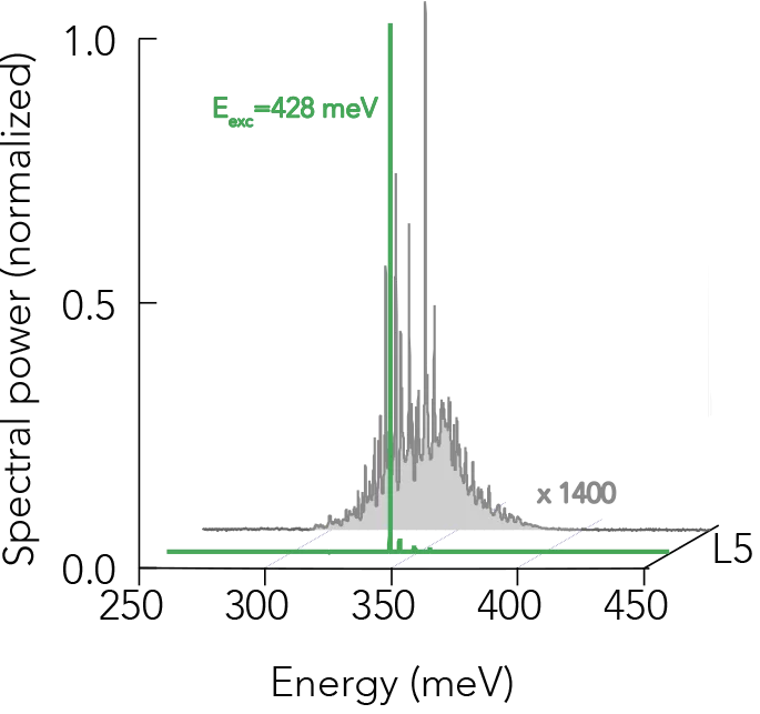
Now, scientists at the Paul Scherrer Institut (PSI) and ETH Zürich, with colleagues from CEA Grenoble, developed a technology to realize for the first time a laser made from elemental, strained Germanium. The current approach of making a Germanium laser using strain was first outlined in 2013 by PSI [1]. Furthermore, back in 2015, the same team demonstrated together with their partners from FZ Jülich, lasing in the alternative GeSn system which, in contrast to elemental Germanium, is a platform with a bandstructure that is intrinsically suited for lasing but more challenging to fabricate [2]. However, the hurdles to make a strained Germanium laser were higher than expected because – as it turned out – the strain at which the bandstructure becomes effective for lasing is higher than predicted. Consequently, Germanium had to be loaded with more strain than anticipated and lasing with very high efficiency and up to temperatures of 100 Kelvin could then be demonstrated [3]. This breakthrough was possible thanks to the high strain achieved, together with a newly employed resonant excitation scheme – light pulses short enough to prepare carriers at the so-called Γ point with nearly perfect radiative properties. This achievement represents the first unequivocal demonstration of lasing in elemental Germanium and defines a path for future Silicon-compatible lasers development.
Based on the obtained insights into the fabrication of strained semiconductors and the relation between strain and the electronic band structure, the PSI team and collaborators will continue working towards the ultimate goal, namely the realization of a practical, room-temperature laser source that is compatible with Silicon technology.
Contacts
Francesco Armand Pilon
Laboratory of Micro- and Nanotechnology
Paul Scherrer Institut, Forschungstrasse 111, 5232 Villigen PSI, Switzerland
Telephone: +41 56 310 4308, email: francesco.armand-pilon@psi.ch [English, Italian]
Dr. Hans Sigg
Laboratory of Micro- and Nanotechnology
Paul Scherrer Institut, Forschungstrasse 111, 5232 Villigen PSI, Switzerland
Telephone: +41 56 310 4048, email: hans.sigg@psi.ch [English, German]
Original Publication
Lasing in strained germanium microbridges
Francesco T. Armand Pilon, Alexey Lyasota, Yann-Michel Niquet, Vincent Reboud, Vincent Calvo, Nicolas Pauc, Julie Widiez, Christopher Bonzon, Jean-Michel Hartmann, Alexei Chelnokov, Jérôme Faist & Hans Sigg
Nature Communications 10(1) 2019
DOI: 10.1038/s41467-019-10655-6