Direkt zum Inhalt
  • Paul Scherrer Institut PSI
  • PSI Research, Labs & User Services

Digital User Office

  • Digital User Office
  • DE
  • EN
  • FR
Paul Scherrer Institut (PSI)
Suche
Paul Scherrer Institut (PSI)

Hauptnavigation

  • Research at PSIÖffnen dieses Hauptmenu Punktes
    • Research Initiatives
    • Ethics and Research integrity
    • Scientific Highlights
    • Scientific Events
    • Scientific Career
    • PSI-FELLOW
    • PSI Data Policy
  • Research Divisions and LabsÖffnen dieses Hauptmenu Punktes
    • Overview
    • Research with Neutrons and Muons
    • Photon Science
    • Energy and Environment
    • Nuclear Energy and Safety
    • Biology and Chemistry
    • Scientific Computing, Theory and Data
    • Large Research Facilities
  • Facilities and InstrumentsÖffnen dieses Hauptmenu Punktes
    • Overview
    • Large Research Facilities
    • Facilities
    • PSI Facility Newsletter
  • PSI User ServicesÖffnen dieses Hauptmenu Punktes
    • User Office
    • Methods at the PSI User Facilities
    • Proposals for beam time
    • Proposal Deadlines
    • Data Analysis Service (PSD)
    • EU support programmes
  • New ProjectsÖffnen dieses Hauptmenu Punktes
    • SLS 2.0
    • IMPACT
  • DE
  • EN
  • FR

Digital User Office (mobile)

  • Digital User Office

Sie befinden sich hier:

  1. PSI Home
  2. Labs & User Services
  3. NUM
  4. LMX
  5. Thin Films and Interfaces
  6. News & Highlights

Sekundäre Navigation

Thin Films and Interfaces Group

  • About the TFI Group
    • Collaborations
    • Funding
  • People
    • Alumni
    • Visitors
  • Research
    • Thin Films - Methods
    • Plasma and Thin Film Analysis
    • Multiferroic Thin Films
    • Renewable Energy Applications
      • Ion Conductors
      • Thin Film Materials for Catalysis
    • Concluded Projects
      • Laser Induced Forward Transfer
      • Li-Metal Oxides
      • Structuring
      • Photo-Interactions with Polymers
    • Current Research Highlights
  • Instrumentation and Services
    • Instrumentation
      • Seifert Booking Page
    • Service for Industry
  • Seminars
    • Seminars 2022
    • Seminars 2021
    • Seminars 2020
    • Seminars 2019
    • Seminars 2018
    • Seminars 2017
    • Seminars 2016
    • Seminars 2015
    • Seminars 2014
    • Seminars 2013
    • Seminars 2012
    • Seminars 2011
    • Former Guest Speakers
  • Conferences
  • Teaching and Education
    • Micro- and Nanostructures
    • Inorganic Thin Films
    • Open Positions
  • News & Highlights Ausgeklappter Submenü Punkt
    • News
    • Highlights 2020
    • Highlights 2019
    • Highlights 2018
    • Highlights 2017
    • Highlights 2016
    • Highlights 2015
    • Highlights 2014
    • Highlights 2013
    • Highlights 2012
  • Publications
    • Papers
    • Books
    • PhD Theses
  • Nützliche Links

  • Laboratory for Multiscale materials eXperiments
  • Laboratory for Neutron Scattering and Imaging
  • PSI Telefon Directory
  • Most Recent Publication
  • Student Projects

Info message

Dieser Inhalt ist nicht auf Deutsch verfügbar.

Scientific Highlights

Scientific Highlights

Toggle filters
Datum
4. November 2013
Polarisierte Neutronen beider Spinausrichtungen up (blau) und down (rot) gelangen unter sehr kleinen Einfallswinkeln in eine Probe. Dort werden sie an den im Magnetfeld H ausgerichteten Momenten gestreut, hier dargestellt für eine Grenzfläche. Aus den gemessenen Unterschieden der Winkelabhängigkeit für beide Spinrichtungen lässt sich ein magnetisches Tiefenprofil ableiten.

Magnetismus im Stress: Gleichzeitiger Anti- und Ferromagnetismus

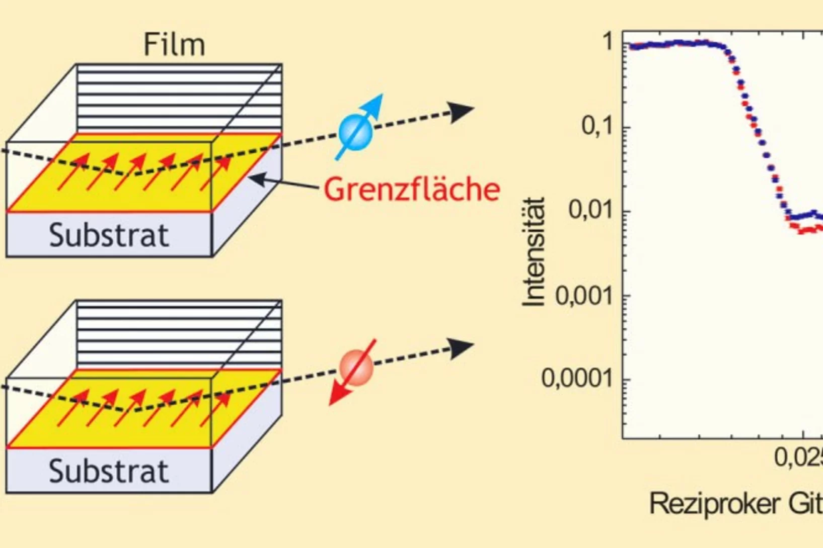
Die gleichzeitige Existenz von Magnetismus und Ferroelektrizät in einem Material ist selten. Setzt sich dieser Magnetismus aus mehreren unabhängigen, magnetischen Grundzuständen zusammen, ist das ungewöhnlich. Einer schweizerisch-französischen Zusammenarbeit unter Leitung des Paul Scherrer Instituts ist es gelungen, mehrere magnetische Grundzustände in einem Material zu realisieren und detailliert zu untersuchen.

Weiterlesen
24. Oktober 2013
Photograph (a) and schematic cross section (b) of a typical Au–LaAlO3–SrTiO3 tunnel device. The broad gold ring (inner diameter, 160 μm) lies on top of the LaAlO3 layer, which serves as a tunnel barrier between the 2DEL and the Au. The outer ring and the centre contact of the device are Au-covered Ti contacts to the 2DEL. c, Cross-sectional high-angle annular dark-field STEM image of a Au–LaAlO3–SrTiO3 tunnel junction. The image is taken along the zone axis of the perovskite unit cells. a.u., arbitrary uni…

Interface superconductor with gap behaviour like a high-temperature superconductor

The physics of the superconducting state in two-dimensional (2D) electron systems is relevant to understanding the high-transition-temperature copper oxide superconductors and for the development of future superconductors based on interface electron systems. But it is not yet understood how fundamental superconducting parameters, such as the spectral density of states, change when these superconducting electron systems are depleted of charge carriers.

Weiterlesen
17. Juli 2013
Diagram of the processes in the LuMnO3 layers studied. The layer is highly strained close to the substrate, which leads to a ferromagnetic (FM) order there. As the distance grows, the strain decreases so that two antiferromagnetic (AFM) orders appear: the spin spirals and the E-type, where two spins point in one direction and the next two in the other.

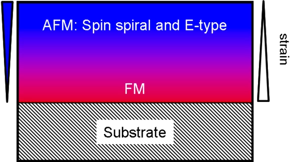
Strain-Induced Ferromagnetism in Antiferromagnetic LuMnO3 Thin Films

Single phase and strained LuMnO3 thin films are discovered to display coexisting ferromagnetic and antiferromagnetic orders. A large moment ferromagnetism (≈1μB), which is absent in bulk samples, is shown to display a magnetic moment distribution that is peaked at the highly strained substrate-film interface. We further show that the strain-induced ferromagnetism and the antiferromagnetic order are coupled via an exchange field, therefore demonstrating strained rare-earth manganite thin films as promising candidate systems for new multifunctional devices.

Weiterlesen
14. April 2013
HAADF STEM micrographs of YSZ thin films deposited by different methods. a) 8YSZ SP (Tdep = 370 °C; Tpa = 600 °C, 20 h), b) 8YSZ AA-CVD (Tdep = 450 °C, Tpa = 600 °C, 20 h), c) 8YSZ AA-CVD (Tdep = 600 °C, Tpa = 600 °C for 20 h), d) 3YSZ PLD (Tdep = 450 °C, pO2 = 7 Pa, Tpa = 600 °C, 1 h) with top and bottom electrode, e) 3YSZ PLD (Tdep = 450 °C, pO2 = 1 Pa, Tpa = 600 °C, 1 h), and f) 8YSZ PLD (Tdep = 700 °C, pO2 = 2.7 Pa, Tpa = 600 °C, 20 h) with top and bottom electrodes.

On Proton Conductivity in Porous and Dense Yttria Stabilized Zirconia at Low Temperature

The electrical conductivity of dense and nanoporous zirconia-based thin films is compared to results obtained on bulk yttria stabilized zirconia (YSZ) ceramics. Different thin film preparation methods are used in order to vary grain size, grain shape, and porosity of the thin films. In porous films, a rather high conductivity is found at room temperature which decreases with increasing temperature to 120 °C. This conductivity is attributed to proton conduction along physisorbed water (Grotthuss mechanism) at the inner surfaces.

Weiterlesen
29. März 2013

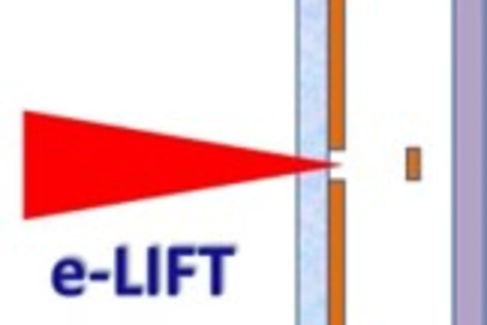
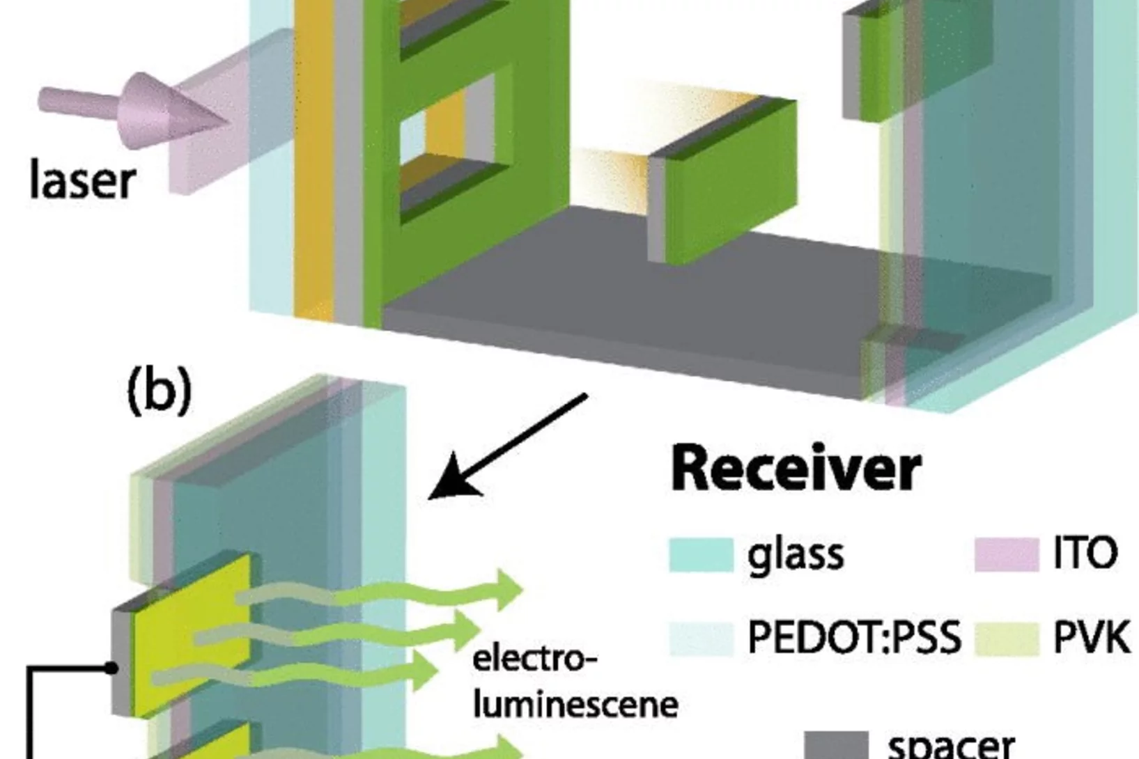
Applications of laser printing for organic electronics

The development of organic electronic requires a non contact digital printing process. The European funded e-LIFT project investigated the possibility of using the Laser Induced Forward Transfer (LIFT) technique to address this field of applications. This process has been optimized for the deposition of functional organic and inorganic materials in liquid and solid phase, and a set of polymer dynamic release layer (DRL) has been developed to allow a safe transfer of a large range of thin films.

Weiterlesen
27. März 2013
(a), (b) IR spectra showing the T dependence of the R mode in a SrTi18O3 single crystal with a ferroelectric transition at TCurie=23  K. (c), (d) Corresponding spectra of quantum paraelectric SrTi16O3.

Electric-Field-Induced Polar Order and Localization of the Confined Electrons in LaAlO3/SrTiO3 Heterostructures

With ellipsometry, x-ray diffraction, and resistance measurements we investigated the electric-field effect on the confined electrons at the LaAlO3/SrTiO3 interface. We obtained evidence that the localization of the electrons at negative gate voltage is induced, or at least enhanced, by a polar phase transition in SrTiO3 which strongly reduces the lattice polarizability and the subsequent screening. In particular, we show that the charge localization and the polar order of SrTiO3 both develop below ∼50  K and exhibit similar, unipolar hysteresis loops as a function of the gate voltage.

Weiterlesen
23. Januar 2013
A scheme showing the LIFT process. The laser beam punching out an Alq3 pixel for transfer from the donor to the receiver substrate is shown in (a), and pair of electroluminescent pixels are shown with a bias applied in(b).

The fabrication of small molecule organic light-emitting diode pixels by laser-induced forward transfer

Laser-induced forward transfer (LIFT) is a versatile organic light-emitting diode (OLED) pixel deposition process, but has hitherto been applied exclusively to polymeric materials. Here, a modified LIFT process has been used to fabricate small molecule Alq3 organic light-emitting diodes (SMOLEDs). Small molecule thin films are considerably more mechanically brittle than polymeric thin films, which posed significant challenges for LIFT of these materials.

Weiterlesen

Mit Sidebar

Contact

Thin Films and Interfaces Group
Paul Scherrer Institut
5232 Villigen PSI
Switzerland
Homepage

Professor Dr. Dr. h.c. Thomas Lippert
Head of Group
OFLB/U110
tel: +41 56 310 4076
fax: +41 56 310 2688
thomas.lippert@psi.ch

Seminars

Thin Films and Interfaces Group Seminars
ENE Seminars
CMT seminar/journal club

Homepage NUM

Research with Neutrons and Muons NUM Division at PSI


PSI Scientific Reports

Archive 2006-2012. The Scientific Reports – containing accounts of research topics from all the different areas – provide an impression of the variety of subjects researched at PSI.


Open Positions

Job Opportunities at Research Division NUM.
top

Fussbereich

Paul Scherrer Institut

Forschungsstrasse 111
5232 Villigen PSI
Schweiz

Telefon: +41 56 310 21 11
Telefax: +41 56 310 21 99

Der Weg zu uns
Kontakt

Besucherzentrum psi forum
Schülerlabor iLab
Zentrum für Protonentherapie
PSI Bildungszentrum
PSI Guest House (in english)
PSI Gastronomie
psi forum-Shop


Service & Support

  • Telefonbuch
  • User Office
  • Accelerator Status
  • Publikationen des PSI
  • Lieferanten
  • E-Rechnung
  • Computing
  • Sicherheit

Karriere

  • Arbeiten am PSI
  • Stellenangebote
  • Aus- und Weiterbildung
  • Career Center
  • Berufsbildung
  • PSI Bildungszentrum

Für die Medien

  • Das PSI in Kürze
  • Zahlen und Fakten
  • Mediacorner
  • Medienmitteilungen
  • Social Media

Folgen Sie uns: Twitter (deutsch) LinkedIn Youtube Facebook Instagram Issuu RSS

Footer legal

  • Impressum
  • Nutzungsbedingungen
  • Editoren-Login