

For solid-state quantum computing the ability to deterministically confine donors in a semiconductor is crucial, not only to create quantum bits defined by the electron or nuclear spin of a dopant, but also to fabricate control systems such as gates mediated by one-dimensional wires or two-dimensional “delta” (∂) layers.

In this project low-dimensional devices are made by confining group V donors in Si. The devices are then investigated electrically by low temperature magnetoresistance measurements and optically by using techniques, such as Fourier transform infrared (FTIR) and time-domain THz spectroscopy. This allows to understand characteristics of the donor electrons in the Si crystal such as interactions between dopant atoms, the spin-orbit and spin-spin coupling, the metal-insulator transition, and their dependence on dopant species. The goal is to reduce the dimensionality of the confinement to one and zero dimensions and to create ordered single-atom arrays, as well as to measure their quantum electro-optic properties.
Recent publications & preprints
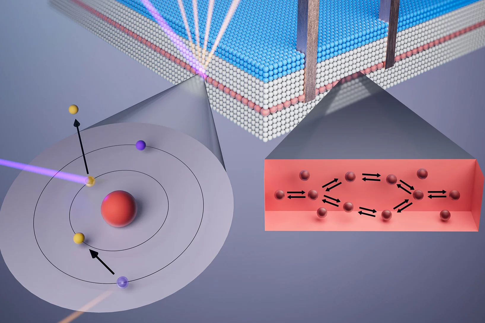
Rapid high-temperature initialisation and readout of spins in silicon with 10 THz photons
A. G. McConnell, N. Dessmann, W. Adamczyk, B. N. Murdin, L. Amato, N. V. Abrosimov, S. G. Pavlov, G. Aeppli, G. Matmon
arXiv:2601.21880
Strong electron-electron interactions in a dilute weakly-localized metal near a metal-to-insulator transition
N. D'Anna, J. Bragg, A. G. McConnell, J. Vonka, P. C. Constantinou, J. Li, S. Fearn, T. J. Z. Stock, S. R. Schofield, N. J. Curson, Y. Soh, M. Bartkowiak, S. Gerber, M. Müller, G. Matmon, G. Aeppli
arXiv:2508.02793
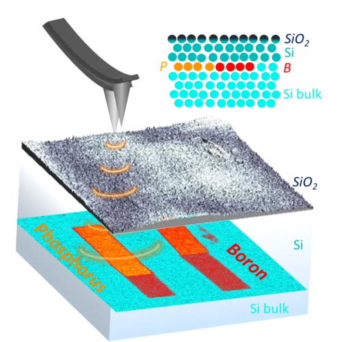
Element-specific, non-destructive profiling of layered heterostructures
N. D'Anna, J. Bragg, E. Skoropata, N. Ortiz Hernández, A. G. McConnell, M. Clémence, H. Ueda, P. C. Constantinou, K. Spruce, T. J. Z. Stock, S. Fearn, S. R. Schofield, N. J. Curson, D. Ferreira Sanchez, D. Grolimund, U. Staub, G. Matmon, S. Gerber, G. Aeppli
arXiv:2410.00241
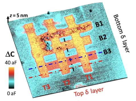
Non-destructive X-ray imaging of patterned delta-layer devices in silicon
N. D'Anna, D. Ferreira Sanchez, G. Matmon, J. Bragg, P. C. Constantinou, T. J.Z. Stock, S. Fearn, S. R. Schofield, N. J. Curson, M. Bartkowiak, Y. Soh, D. Grolimund, S. Gerber, G. Aeppli
Advanced Electronic Materials 2023, 2201212 (2023)
Recent highlights

Project members


Head of Laboratory for X-ray Nanoscience and Technologies (LXN)

Senior scientist
Condensed Matter Theory Group >>
Building/Room: WHGA/136

Head of PSI Center for Photon Science