Direkt zum Inhalt
  • Paul Scherrer Institut PSI
  • PSI Research, Labs & User Services

Digital User Office

  • Digital User Office
  • DE
  • EN
  • FR
Paul Scherrer Institut (PSI)
Suche
Paul Scherrer Institut (PSI)

Hauptnavigation

  • Research at PSIÖffnen dieses Hauptmenu Punktes
    • Research Initiatives
    • Ethics and Research integrity
    • Scientific Highlights
    • Scientific Events
    • Scientific Career
    • PSI-FELLOW
    • PSI Data Policy
  • Research Divisions and LabsÖffnen dieses Hauptmenu Punktes
    • Overview
    • Research with Neutrons and Muons
    • Photon Science
    • Energy and Environment
    • Nuclear Energy and Safety
    • Biology and Chemistry
    • Scientific Computing, Theory and Data
    • Large Research Facilities
    • Logistics
  • Facilities and InstrumentsÖffnen dieses Hauptmenu Punktes
    • Overview
    • Large Research Facilities
    • Facilities
    • PSI Facility Newsletter
  • PSI User ServicesÖffnen dieses Hauptmenu Punktes
    • User Office
    • Methods at the PSI User Facilities
    • Proposals for beam time
    • Proposal Deadlines
    • Data Analysis Service (PSD)
    • EU support programmes
  • New ProjectsÖffnen dieses Hauptmenu Punktes
    • SLS 2.0
    • IMPACT
  • DE
  • EN
  • FR

Digital User Office (mobile)

  • Digital User Office

Sie befinden sich hier:

  1. PSI Home
  2. Labs & User Services
  3. PSD
  4. LNQ
  5. Research Groups
  6. Nanotechnology Group

Sekundäre Navigation

Laboratory for Nano and Quantum Technologies

  • About LNQ
    • Organisational Structure
  • People
  • Research Groups Ausgeklappter Submenü Punkt
    • Nanotechnology Group Ausgeklappter Submenü Punkt
      • People
      • Research Projects
    • Quantum Engineering
      • People
      • Research Projects
    • Advanced Nanomanufacturing
      • People
      • Research Projects
        • Three dimensional surface topographies
        • Nanoimprint Lithography
      • Scientific Highlights and News
    • Superconducting Quantum Circuits Group
      • People
      • Scientific Highlights and News
    • Bosonic Quantum Information
      • People
      • Open positions
      • Scientific Highlights and News
    • Ion Trap Quantum Computing
      • Open Positions
      • People
      • Publications
    • Photonics – INPhO
      • People
  • Facilities and Equipment
    • ETHZ-PSI Quantum Computing Hub
    • Cleanroom Laboratories
    • Nanoimprint Lithography Facilities
    • Scanning Electron Microscopy
  • Scientific Highlights and News
    • Archive
  • Publications

Info message

Dieser Inhalt ist nicht auf Deutsch verfügbar.
nanotechnology

Nanotechnology

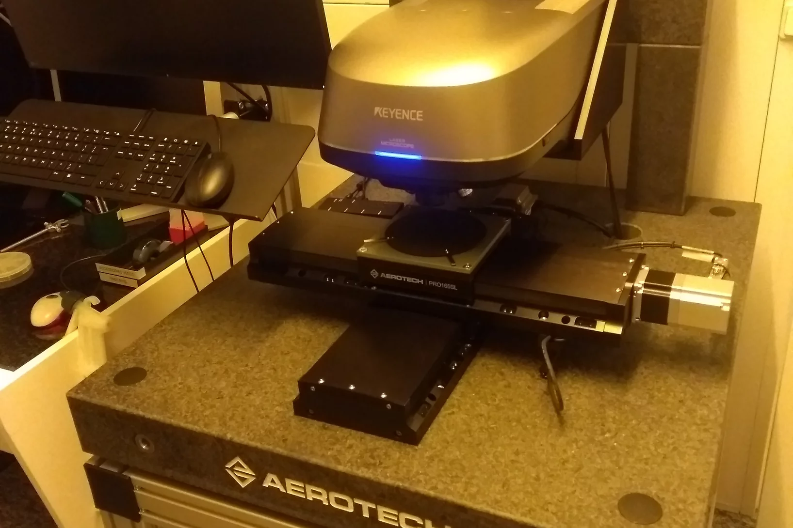
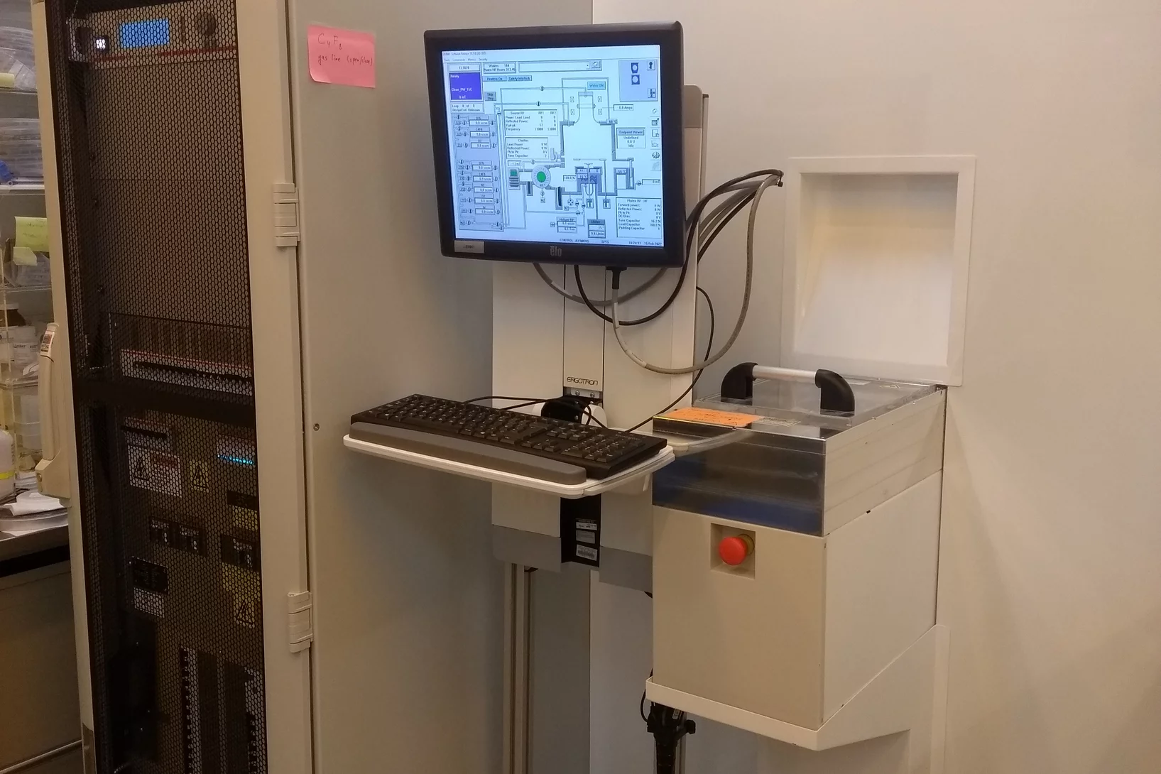
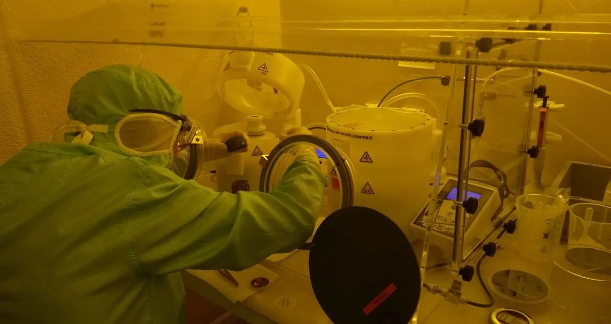
The mission of the Nanotechnology group is to operate the cleanrooms at the Laboatory for Nano and Quantum Technologies, to provide scientific and technological support to the cleanroom users and to develop novel micro- and nanofabrication techniques for success of current and future research projects. Moreover, the group is also providing nanofabication services to external academic and industrial customers.


Scientific Highlights and News

15. November 2022

Nanotechnology group is welcoming Kevin Hofhuis

Starting in Novemeber 2022, Dr. Kevin Anthony Hofhuis joined the Nanotechnology group as an E-beam Lithography Scientist.

Welcome to the cleanroom team, Kevin!

Weiterlesen
15. November 2021
Keyence optical 3D Profiler

New Confocal Microscope Keyence VK-X3100

Keyence VK-X3100 is a  non-contact 3D surface profiler. It enables capturing images and performing the profile, roughness and film thickness analysis. The measurement head is equipped with semiconductor laser with the wave length of 404 nm and white LED. To reach the best performance, it uses laser confocal scanning, focus variation, adn while light interferometry  measurement methods. The motorized sample stage allows for automatic inspection of up to 200mm wafers.

Weiterlesen
12. Oktober 2020
Heidelberg DWL66+ at LMN

Installation of Heidelberg DWL66+

Heidelberg DWL66+ direct laser writer, funded by ANAXAM, is in operation now. It is a new photolithographic system closing the gap between the mask aligners on one side and the Nanoscribe two-photon 3D lithography system on the other. It is equipped with semiconductor laser with the wave length of 405 nm and is capable of exposing the minimum feature size down to 0.3 µm on wafers up to 200 mm or 9"x9" mask blanks.

Weiterlesen
14. September 2020
SPTS Rapier DRIE

Installation of SPTS Rapier Deep Reactive Ion Etcher

SPTS Rapier system for Si deep reactive ion etching (DRIE) is released for user operation. The system is acquired by PSI as a part of SNF R’Equip project “Advanced Si DRIE tool for highly uniform ultra-deep structuring (SiDRY)”. This versatile tool is equipped with pulsed bias option and sensitive ClaritasTM optical end point detection system. Electrostatic clamping and wafer edge protection systems are both available for three wafer diameters – 100 mm, 150 mm, and 200 mm.

Weiterlesen

Mit Sidebar

Contact

Dr. Vitaliy Guzenko

Laboratory for Nano and Quantum Technologies
Paul Scherrer Institut
5232 Villigen PSI
Switzerland

Telephone: +41 56 310 5436
E-mail: vitaliy.guzenko@psi.ch
top

Fussbereich

Paul Scherrer Institut

Forschungsstrasse 111
5232 Villigen PSI
Schweiz

Telefon: +41 56 310 21 11
Telefax: +41 56 310 21 99

Der Weg zu uns
Kontakt

Besucherzentrum psi forum
Schülerlabor iLab
Zentrum für Protonentherapie
PSI Bildungszentrum
PSI Guest House (in english)
PSI Gastronomie
psi forum-Shop


Service & Support

  • Telefonbuch
  • User Office
  • Accelerator Status
  • Publikationen des PSI
  • Lieferanten
  • E-Rechnung
  • Computing
  • Sicherheit

Karriere

  • Arbeiten am PSI
  • Stellenangebote
  • Aus- und Weiterbildung
  • Career Center
  • Berufsbildung
  • PSI Bildungszentrum

Für die Medien

  • Das PSI in Kürze
  • Zahlen und Fakten
  • Mediacorner
  • Medienmitteilungen
  • Social Media

Folgen Sie uns: Twitter (deutsch) LinkedIn Youtube Facebook Instagram Issuu RSS

Footer legal

  • Impressum
  • Nutzungsbedingungen/Datenschutz
  • Editoren-Login