Aller au contenu principal
  • Paul Scherrer Institut PSI
  • PSI Research, Labs & User Services

Digital User Office

  • Digital User Office
  • DE
  • EN
  • FR
Paul Scherrer Institut (PSI)
Rechercher
Paul Scherrer Institut (PSI)

Hauptnavigation

  • Research at PSIOuvrir ce point de menu principal
    • Research on Covid-19
    • Research Initiatives
    • Ethics and Research integrity
    • Scientific Highlights
    • Scientific Events
    • Scientific Career
    • PSI-FELLOW
    • PSI Data Policy
  • Research Divisions and LabsOuvrir ce point de menu principal
    • Overview
    • Research with Neutrons and Muons
    • Photon Science
    • Energy and Environment
    • Nuclear Energy and Safety
    • Biology and Chemistry
    • Scientific Computing, Theory and Data
    • Large Research Facilities
  • Facilities and InstrumentsOuvrir ce point de menu principal
    • Overview
    • Large Research Facilities
    • Facilities
    • PSI Facility Newsletter
  • PSI User ServicesOuvrir ce point de menu principal
    • User Office
    • Methods at the PSI User Facilities
    • Proposals for beam time
    • Proposal Deadlines
    • Data Analysis Service (PSD)
    • EU support programmes
  • New ProjectsOuvrir ce point de menu principal
    • SLS 2.0
    • IMPACT
  • DE
  • EN
  • FR

Digital User Office (mobile)

  • Digital User Office

Vous êtes ici:

  1. PSI Home
  2. Labs & User Services
  3. PSD
  4. LXN
  5. Facilities and Equipment
  6. Electron Beam Lithography

Navigation secondaire

Laboratory for X-ray Nanoscience and Technologies (LXN)

  • About LXN
    • Organisational Structure
  • Open Positions
  • People
  • Research Groups
    • X-ray Nano-Optics
      • X-ray Optics for Imaging and Spectroscopy
        • Fresnel Zone Plate for X-ray Microscopy
        • Blazed X-ray Optics
        • Zernike X-ray Phase Contrast Microscopy
        • Fresnel Zone Plates for RIXS
        • Refractive Lenses by 2 Photon 3D Lithography
      • Wavefront Metrology and Manipulation
        • Vortex Fresnel Zone Plates
        • Grating-based Wavefront Metrology
      • X-ray Optics for XFELs
        • Diamond Fresnel Zone Plates
        • Beam Splitter Gratings for Spectral Monitoring
        • A Delay Line for Ultrafast Pump-Probe Experiments
        • X-ray Streaking for Ultrafast Processes
    • Molecular Nanoscience
      • On-surface Chemistry
      • Spins in Molecular Monolayers
      • SiC: Surfaces and Interfaces
      • Our Research Team
    • Advanced Lithography and Metrology
      • EUV Interference Lithography
      • EUV Lensless Imaging
      • ALM Nanoscience
    • Quantum Photon Science
      • News and highlights
      • People
      • Open positions
      • Current projects
        • Bosonic quantum error correction with superconducting circuits
        • Imaging quantum many-body states
        • Nonlinear magnonics
        • Optical devices & methods
        • Rare-earth quantum magnets
        • Rydberg states in Si ∂-layers
        • Strained Ge laser (former research activity of H. Sigg & collaborators)
        • Van der Waals materials & devices
      • Infrastructure
        • Cristallina-Q
        • IR beamline
        • Nano-fabrication
      • Publications
      • QTC@PSI
    • Detectors
      • Projects
        • MYTHEN
        • GOTTHARD
        • EIGER
        • JUNGFRAU
        • MOENCH
        • AGIPD
        • Documentation
        • Software Releases
      • Research
      • Detectors Scientific Highlights
      • Publications
      • Team
  • Facilities and Equipment Sous-menu élargi
    • Surface Science Lab
    • Scanning Electron Microscopy
    • Scanning Probe Microscopy
    • PEARL Beamline
    • XIL Facility at the SLS
    • Cleanroom Labs
  • Scientific Highlights and News
    • Archive
  • Publications
    • Archive

Info message

Ce contenu n'est pas disponible en français.

Electron Beam Lithography

Direct write e-beam lithography tools at LMN provide a variety of powerful techniques for the lateral as well as three-dimensional pattern transfer with the resolution down to 10 nm. Compared to other nanostructuring methods, it stands out for a high level of flexibility and reasonably high patterning speed.

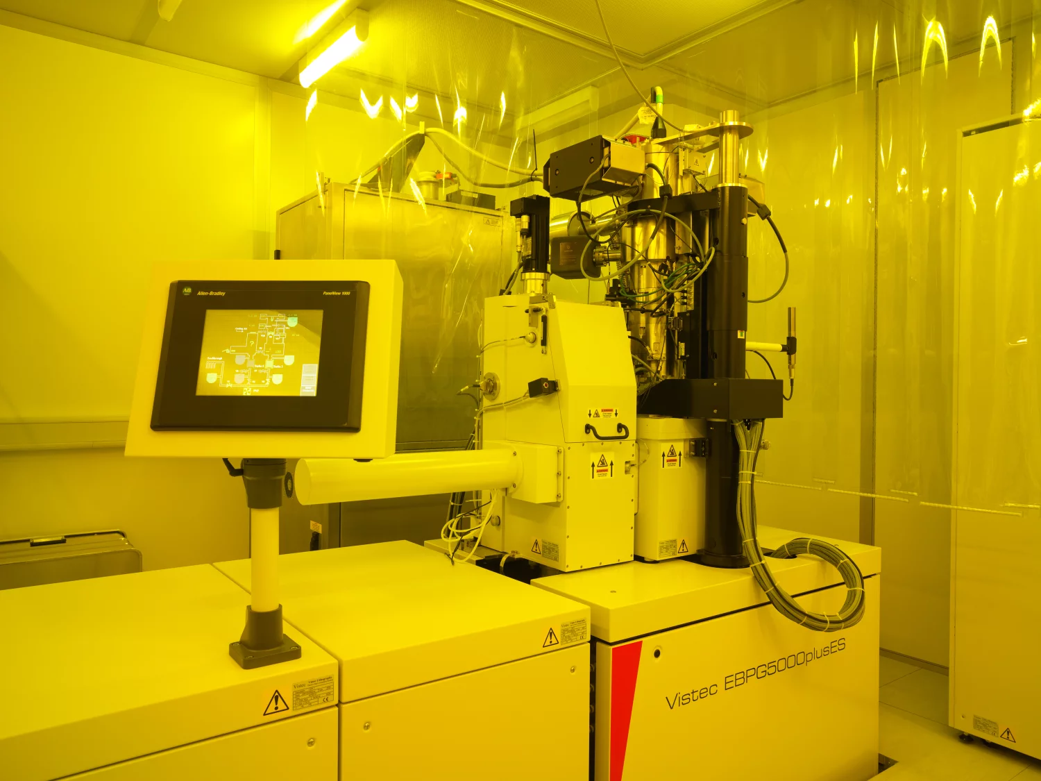
Vistec EBPG 5000PlusES

Vistec EBPG 5000PlusES installed in ODRA/55a
Vistec EBPG 5000Plus e-beam lithography tool is in operation since March 2009. It is installed in a dedicated cleanroom of class 100 with high precision temperature control at 21 ± 0.1° C. This is a prerequisite for the minimization of thermal drift in the electron optics, and thus, for the excellent performance of the system. The main characteristics of the tool are:
  • It is a vector-scan direct write tool with a Gaussian shaped beam. The beam scanning is controlled by combination of two deflection systems. Thus, the maximum writing field size of 512×512 µm² in conjunction with the beam stepping frequencies up to 50 MHz are achievable.
  • The spot can be focused to less than 5 nm in diameter. Owing to the wide range of available beam currents (200 pA – 200 nA), the high-throughput as well as high-resolution exposures are possible.
  • It is operated at 100 keV acceleration voltage. Up to several micrometers thick layers of e-beam resist can be exposed with small forward scattering.
  • Wafers with diameter up to 150 mm and mask blanks up to 5×5 sq. inch can be processed.
  • The overlay precision (mean + 3σ) is below 40 nm for the largest and 20 nm for smaller (100×100 µm²) write fields.
  • For the conversion of the CAD patterns into machine specific format, including proximity effect correction (PEC), a special software solution – Layout BEAMER – is used. In some special cases, a direct coding of the beam movement is advantageous, which allows up to speed up remarkable the exposure or improve further the resolution.
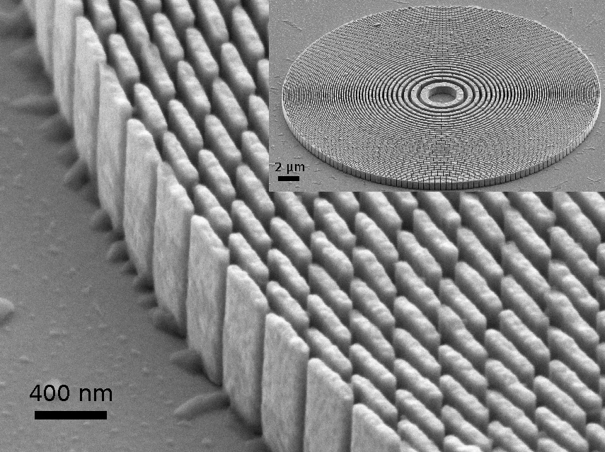
Fresnel zone plate (Gold, electroplating in PMMA mold)
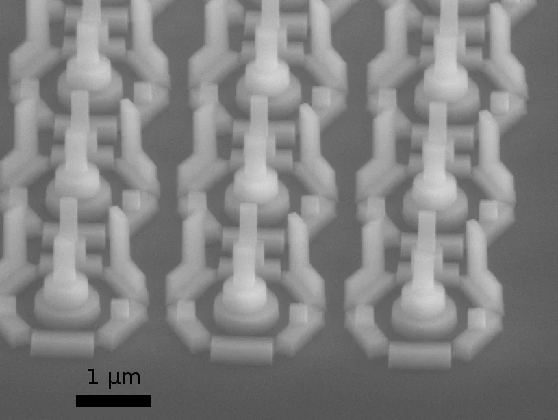
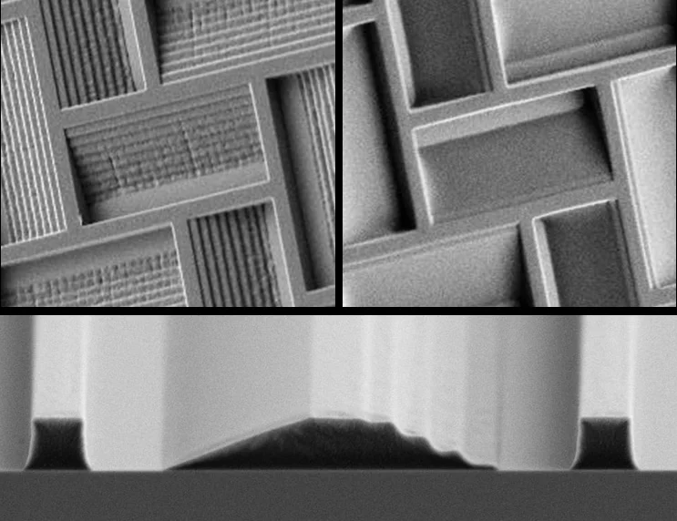
Multilayer HSQ structures (overlay exposures)

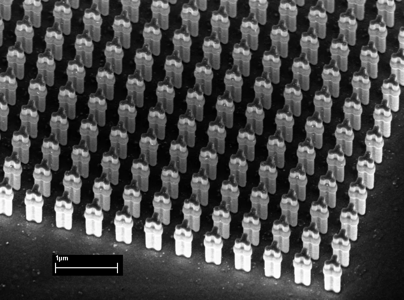
Artificial 2D crystal made of high aspect ratio structures (Gold, electroplating in a PMMA mold)
3D Topological profiles in 1 µm thick PMMA layer

Sidebar

Contact

User Support and Scientific Advice
 
Dr. Vitaliy Guzenko
Telephone: +41 56 310 54 36
E-mail: vitaliy.guzenko@psi.ch
top

Pied de page

Paul Scherrer Institut

Forschungsstrasse 111
5232 Villigen PSI
Suisse

Téléphone: +41 56 310 21 11
Téléfax: +41 56 310 21 99

Comment nous trouver 
Contact

Centre de visiteurs psi forum
Laboratoire élèves iLab (en allemand)
Centre de protonthérapie
Centre de Formation du PSI (en allemand)
PSI Guest House (en anglais)
PSI Gastronomie (en allemand)
psi forum shop

Service & Support

  • Annuaire
  • User Office
  • Accelerator Status
  • Publications du PSI
  • Fournisseurs
  • E-facture
  • Computing (en anglais)
  • Sicherheit (en allemand)

Carrière

  • Travailler au PSI
  • Offres d'emploi
  • Formation initiale et formation continue
  • Formation professionnelle (en allemand)
  • Centre de Formation du PSI

Pour les médias

  • Le PSI en bref
  • Chiffres et faits
  • Le coin médias
  • Communiqués de presse
  • Social Media

Suivez le PSI: Twitter (en allemand) LinkedIn Youtube Issuu RSS

Footer legal

  • Impressum
  • Conditions d'utilisation
  • Login éditeurs