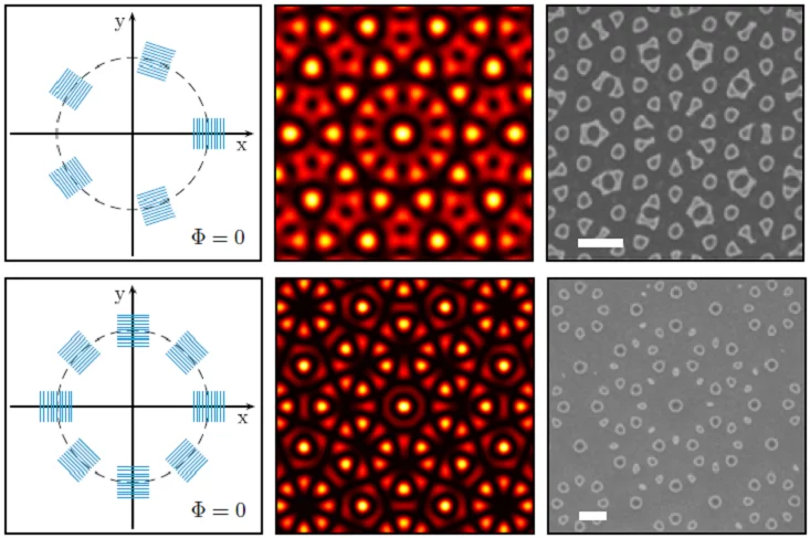
High resolution Nanostructures
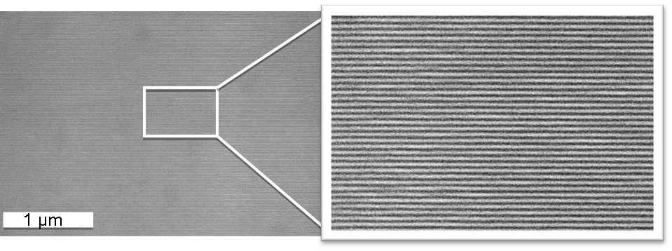
XIL-II, the EUV-IL tool at SLS provides the smallest patterns ever written with photons. The resolution is mainly limited by resists and mask writing.
Versatile Nanostructures
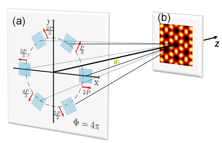
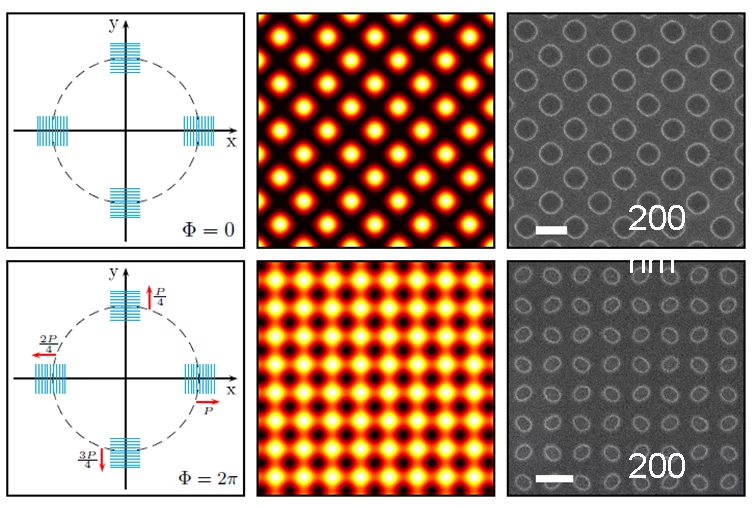
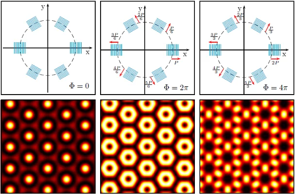
Versatile periodic nanostructures can be obtained by changing the number of interfering beams and by controlling the relative phases of the beams. The phase control is achieved by controlling the relative positions of the gratings in the mask design and fabrication. This opens up the potential to generate complex periodic as well as quasi-crystal like structures. We have using EUV-IL.11,12 In our recent numerical simulations, we reported that hexagonal arrays of dots and honeycomb structures as well as kagome lattices could be obtained by interference of six beams with well-controlled relative phases.
Large Area Patterning
Large area and high throughput patterning is one of the strengths of EUV-IL. Up to 2x2 mm2 are possible at a single exposure, limited by the beam size and mask area. With a new technique of beam scan exposure, up to 5x5 mm2 are obtained. Using step and repeat technique, nanostructures over an area of up to 80x80 mm2 can be obtained, but with relatively with large stitching errors.

