Laser-Induced Forward Transfer (LIFT)


LIFT single.jpg
The laser induced forward transfer is a direct laser writing, one step process. LIFT can operate under atmospheric conditions, is compatible with low laser fluences, allows the printing of organic and inorganic materials as well as biological elements and the printing can take place from liqud or solid phases. It further has a high lateral resolution only defined by the laser spot size, it is “solvent-free”, highly flexible, and has multilayer capabilities. The following images shows how the transfer of a single layer is typically done. A (UV) laser beam with an apperture defined profile removes and lifts the corresponding area (pixel) out of a continuous layer coated on a (UV) transparent substate. The lifted layer (flyer) is moved onto a receiver substrate.
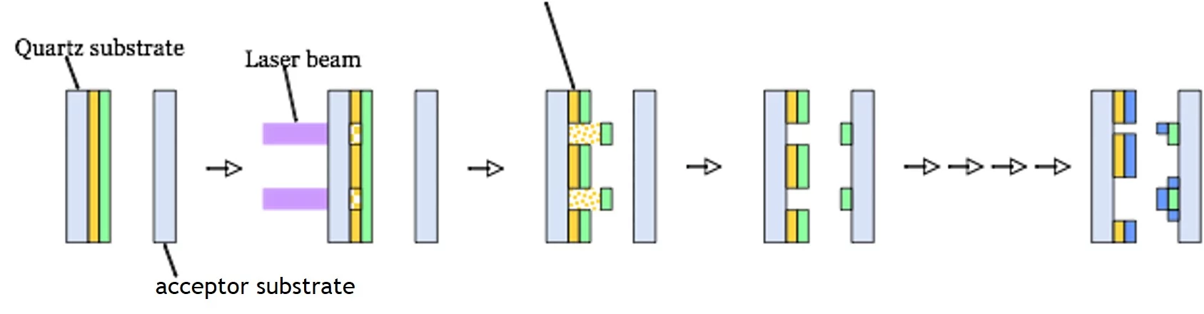
The disadvantage of the materials transfer using light is, the entire process depends on the optical properties of the transferred material. To reduce the dependence on the optical absorption properties, dynamic release layers (DRL) are introduced. These DRL materials are sensitive to the wavelength used for the LIFT process (often UV) and have the benefit that biologically sensitive materials can be transfered with a low thermal impact due to a reduction in the ablation fluence. The following image shows schematically how the LIFT process works with the introduction of a DRL.
LIFT.jpg

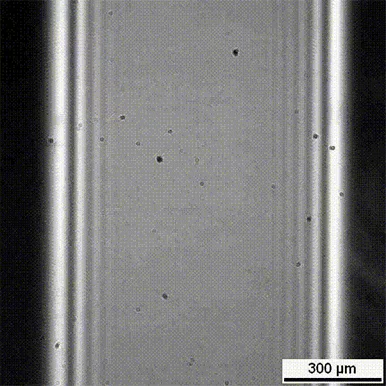
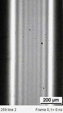
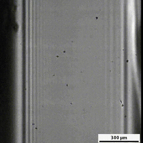
Time-Resolved Imaging


One important aspect in LIFT is a better understanding of the transfer process, which we study in detail by ns-shadowgraphy. A typical sequence of photos for the LIFT process using a dynamic release layer (DRL) and polystyrine as transfer material at ambient conditions is shown in the images.
Next are four examples of solid and liquid material being transfered. Shadowgraphy is used here to understand the transfer conditions which allow or prevent the transfer a functional pixel onto a receiver substrate.

LIFT of a 80 nm thick Al layer in air with 150 nm triazene as DRL and an ablationn fluence of 270 mJ cm-2. The Al layer decomposes before reaching the end of the 1mm air gap because the distance was too long and the shock wave is partially being reflected backwards from the receiver side.

LIFT of a 80 nm thick Al layer in air with 150 nm triazene as DRL and an ablationn fluence of 270 mJ cm-2. The Al layer decomposes before reaching the end of the 0.5 mm air gap as a result of a back-bouncing shock wave.

LIFT of an Al layer transfered at 10-2mbar. There is no shock wave travelling ahead of the flyer, but the flyer is destroyed upon impact with the substrate.

Printing of a liquid dot containing proteins with a DRL. The transfered liquid film is 10 micron thick and moved with 60 mJ cm-2. The printed pixel on the receiver side is 40 µm in diameter as shown in the following image.


Sensor Materials by LIFT

SnO2 Sensors

SnO2 based gas sensors are commercially available and are used to detect volatile organic compounds. Deposition of SnO2 onto these sensors is commonly done by ink-jet printing and a heat treatment to remove solvent residuals. LIFT as a solvent free technique is an ideal candidate to deposit SnO2 onto sensors.
Different approaches were used to prepare the SnO2 LIFT donor substrates. The films were prepared by spin coating commercially available SnO2 nano-particles and tin based metal-complex precursors.

Laser transfers of these materials were performed with and without dynamic release layers onto sensor-like microstructures as shown on the right hand side. The electric conductivity of the transferred pixels was measured at elevated temperatures (~400°C) and varying gas compositions. Experiments have been successfully performed with ethanol concentrations down to 10 ppm in air.

The sensitivity was analyzed in order to find the best precursor system and most suited transfer conditions for a commercial application. Subsequently these systems were transferred onto real sensor structures and tested for their functionality. The LIFT printed sensors were exposed to low concentration of ethanol and methane in air and the response was compared to the commercial sensors based on the same design. The LIFT printed sensors showed an up to four time higher sensitivity than the commercial sensors.
LIFT printed SnO2 sensor and schematics of a Microsens gas sensor

Polymer Sensors

(with the the Photonic Processing of Advanced Materials Group at the National Institute for Laser, Plasma and Radiation Physics in Bucharest and the CNR – Istituto di Acustica “O.M. Corbino”, (IDAC – CNR), Rome)


a) Optical microscopy images of a) PIB, b) PECH, and c) PEI polymers transferred by LIFT onto 2-port SAW devices. b) Schematic drawing of the SMR (left side) and optical microscopy images of SMR devices coated with PEI polymer deposited at 400 (left) and 300 (right) mJ/cm2 laser fluence.
a) Time response of the three sensors for two concentrations of EtOAc. b) Response curve for PECH, PEI, and PIB sensors upon exposure to different concentrations of DMMP.
The present project aims at the development of novel fabrication methods for the deposition of patterned single or multilayer thin-film architectures based on mild, “solvent-free” or “dry” material transfer techniques, such as the Laser Induced Forward Transfer. The technique can also be used to deposited multi-layers of polymers or other materials which can not be done using solvent based-methods. These pixels will be the active layers in new developed SAW (surface acoustic wave) and BAW-TFBAR (bulk acoustic wave-thin film bulk acoustic wave resonator) electro-acoustic devices. These sensors can be used as chemical sensor for organic compounds based on chemical selective polymeric materials, as biosensor based on proteins or as gas sensor based on semiconducting oxides and/or catalysts.

OLED Materials by LIFT

(with the Laboratory for Functional Polymers, Empa)


Flatter and flatter screens and increasingly luminous and brilliant colour displays characterise the appearance of modern electronic devices. A next innovation step will be the development of flexible plastic displays which are not anymore based on rigid carriers. Innovative laser-based microfabrication techniques, such as LIFT, open up new possibilities for ‘plastic electronics’ which will allow to deposit different materials in one layer with a high lateral resolution without any influence of the solvents (in principle).

Experimental approach for the deposition of polymer OLED pixels: Layer architecture of the donor and receiver substrate for the pixel transfer of an OLED material: A transparent indium-tin-oxide (ITO) anode, a thin layer (20 – 40 nm) of the electroluminescent polymer MEH-PPV, an aluminum cathode (70 nm), and a aryltriazene photopolymer film (100 nm). The incident laser pulse decomposes the sacrificial photopolymer layer and catapults the bilayer system MEH-PPV/Al in one step towards the receiver surface.
Progress in the transfer of multiple PFO PLED pixels by LIFT. (a) The first transfers of plain blue and green transfers with Ag / Cs2CO3 cathode are shown, (b) the first three colour pixels with a silver cathode, (c) preliminary pixels with an aluminium cathode, (d) optimised pixels with an Al cathode and (e) an Al / TBA cathode. All the pixels were transferred with a fluence of approximately 70 mJ/cm2.
Electroluminescence spectra of tri-colour LIFT pixels with an Al / TBA cathode (a), and with an Al cathode (b). On both graphs the conventionally fabricated devices’ EL spectra are shown with a solid line and a colour corresponding to the relevant device. The blue pixels are represented by the blue squares, the green pixels are green triangles, and the red pixels are red circles. Tricolour pixels imaged using a light microscope are shown in (c) and (d). The pixels in (c) are made using an Al / TBA cathode, and have a bias of 20 V applied across them. The pixels in (d) are made with a plain Al cathode, and have a bias of 24 V.

Biological Materials by LIFT

(with groups from RPI, Empa, the Georgia Institute of Technology, the Hungarian Academy of Sciences and University of Szeged and the National Institute for Laser, Plasma and Radiation Physics in Bucharest)

Tissue engineering integrates biology and materials engineering in developing next-generation medical technologies. Controlling cell adhesion/location, proliferation and patterning is critical in developing next-generation sensing devices and advanced tissue engineered constructs. In depositing sensitive materials such as biomolecules and live cells, the absorption coefficient of the solvent might not be entirely preclude absorption by the biomolecules. Therefore strongly absorbing dynamic release layers are one possible option to protect the biomolecules from UV light.

Confocal micrographs of stained B35 neuroblasts show viable nucleus and cytoskeleton at 24 h post transfer and at (b) 48 h post transfer. The scale for both equals 10 μm.

Other applications

Nanocrystal quantum dots

(with the groups from Empa and Penn State University)

Recently, colloidal semiconductor nanocrystal quantum dots (NQDs) has drawn immense attention in the photonics research community due to their superior optical properties and easy processibility. Semiconductor NQDs are nanocrystals that are smaller in size than the diameter of a Bohr exciton in a bulk crystal of the same material. By reducing the size of the nanocrystal core, the quantum confinement of the electronic states in the NQD is increased, with a consequent increase in the exciton energy. In CdSe nanocrystals, for instance, quantum confinement increases the exciton energy from a bulk bandgap of 1.7 eV to any value up to 2.75 eV, and by controlling the particle size during the synthesis, the peak emission wavelength of CdSe(ZnS) core/shell NQDs can be tuned continuously from 470 nm to 650 nm.

Pictures of an ITO glass plate carrying a 6 × 6 matrix of alternating pixels composed of 5 nm-diameter CdSe(CdS) NQDs (yellow) and 6 nm-diameter NQDs (red) under UV illumination (left) and room light (right) illumination. The nanocrystal emitter matrix was patterned over the ITO glass plate by the LIFT using a triazene polymer as DRL.
Metals and amorphous ceramics

(with the groups from Empa and the University of Southampton)

LIFT with a DRL is also not only useful for sensitive materials, but "hard" materials, such as metals and ceramics can be trasnferred also with high lateral resolution. The application of the DRL and fs laser pulses reveals certain advantages over classical LIFT, where the transfer layer is directly irradiated.

SEM micrographs of GdGaO deposition without a triazene polymer-DRL (≈ 120mJ/cm2) (a), and with the DRL (≈ 90–100mJ/cm2) using a 130 fs laser at 800 nm.
Optical micrographs of Al deposition with a triazene-polymer-DRL (left) and without a DRL using a XeCl excimer laser (308 nm, 20 ns). LIFT with DRL reveals a much better resolution of the Al pixel on the receiver, which has been transferred at much lower fluences.