
Lab News & Scientific Highlights

Alexander Grimm wins 2022 Nicholas Kurti prize
We are happy to announce that Alex has been awarded the 2022 Nicholas Kurti Science prize. The prize recognises his work on non-linear effects in Josephson junctions for quantum information processing.
Capturing control errors in quantum annealing
The real-world application of this type of quantum computing gets one step closer with a new method to capture errors while qubits are talking to each other.
Une solution à l’insoluble
Le PSI et l’ETH Zurich ont créé le Quantum Computing Hub. Des chercheurs de pointe y collaborent au développement d’ordinateurs quantiques.
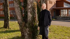
«Lorsqu’on occupe une certaine position, il ne faut pas se cacher»
Kirsten Moselund dirige le nouveau laboratoire des technologies nanométriques et quantiques. En entretien, elle évoque la recherche quantique au PSI et la contribution que pourrait apporter la nanophotonique.
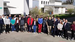
LNQ Kick-off
On April 11th, we had the opportunity to celebrate the kick-off meeting of the new Laboratory of Nano and Quantum Technologies (LNQ), and many had the chance to meet their new colleagues for the first time. Presently, our lab joins together two cleanroom-technology focused groups, Nanotechnology led by Dr. Vitaliy Guzenko and Advanced Nanomanufacturing by Dr. Helmut Schift, respectively, with groups focusing on three different technology platforms in quantum computing. These are Ion trap Quantum Computing led by Dr. Cornelius Hempel, Superconducting Quantum Circuits that is an extension of Prof. Andreas Wallraff's activities at ETHZ, and Neutral Atoms Quantum Engineering, which will be led by Prof. Wenchao Xu joining in August.

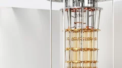
Superconducting qubit first success at Quantum Computing Hub
Andreas Wallraff talks about moving in, refrigerators and measuring the first superconducting qubit at the ETHZ-PSI Quantum Computing hub.
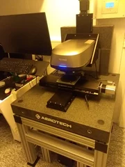
New Confocal Microscope Keyence VK-X3100
Keyence VK-X3100 is a non-contact 3D surface profiler. It enables capturing images and performing the profile, roughness and film thickness analysis. The measurement head is equipped with semiconductor laser with the wave length of 404 nm and white LED. To reach the best performance, it uses laser confocal scanning, focus variation, adn while light interferometry measurement methods. The motorized sample stage allows for automatic inspection of up to 200mm wafers.
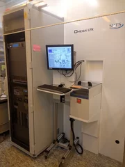
Installation of SPTS Rapier Deep Reactive Ion Etcher
SPTS Rapier system for Si deep reactive ion etching (DRIE) is released for user operation. The system is acquired by PSI as a part of SNF R’Equip project “Advanced Si DRIE tool for highly uniform ultra-deep structuring (SiDRY)”. This versatile tool is equipped with pulsed bias option and sensitive ClaritasTM optical end point detection system. Electrostatic clamping and wafer edge protection systems are both available for three wafer diameters – 100 mm, 150 mm, and 200 mm.