Aller au contenu principal
  • Paul Scherrer Institut PSI
  • PSI Research, Labs & User Services

Digital User Office

  • Digital User Office
  • DE
  • EN
  • FR
Paul Scherrer Institut (PSI)
Rechercher
Paul Scherrer Institut (PSI)

Hauptnavigation

  • Research at PSIOuvrir ce point de menu principal
    • Research Initiatives
    • Ethics and Research integrity
    • Scientific Highlights
    • Scientific Events
    • Scientific Career
    • PSI-FELLOW
    • PSI Data Policy
  • Research Divisions and LabsOuvrir ce point de menu principal
    • Overview
    • Research with Neutrons and Muons
    • Photon Science
    • Energy and Environment
    • Nuclear Energy and Safety
    • Biology and Chemistry
    • Scientific Computing, Theory and Data
    • Large Research Facilities
    • Logistics
  • Facilities and InstrumentsOuvrir ce point de menu principal
    • Overview
    • Large Research Facilities
    • Facilities
    • PSI Facility Newsletter
  • PSI User ServicesOuvrir ce point de menu principal
    • User Office
    • Methods at the PSI User Facilities
    • Proposals for beam time
    • Proposal Deadlines
    • Data Analysis Service (PSD)
    • EU support programmes
  • New ProjectsOuvrir ce point de menu principal
    • SLS 2.0
    • IMPACT
  • DE
  • EN
  • FR

Digital User Office (mobile)

  • Digital User Office

Vous êtes ici:

  1. PSI Home
  2. Labs & User Services
  3. PSD
  4. LNQ
  5. Research Groups
  6. Advanced Nanomanufacturing
  7. Research Projects
  8. Nanoimprint Lithography

Navigation secondaire

Laboratory for Nano and Quantum Technologies

  • About LNQ
    • Organisational Structure
  • People
  • Research Groups Sous-menu élargi
    • Nanotechnology Group
      • People
      • Research Projects
    • Quantum Engineering
      • People
      • Research Projects
    • Advanced Nanomanufacturing Sous-menu élargi
      • People
      • Research Projects Sous-menu élargi
        • Three dimensional surface topographies
        • Nanoimprint Lithography
      • Scientific Highlights and News
    • Superconducting Quantum Circuits Group
      • People
      • Scientific Highlights and News
    • Bosonic Quantum Information
      • People
      • Open positions
      • Scientific Highlights and News
    • Ion Trap Quantum Computing
      • Open Positions
      • People
      • Publications
    • Photonics – INPhO
      • People
  • Facilities and Equipment
    • ETHZ-PSI Quantum Computing Hub
    • Cleanroom Laboratories
    • Nanoimprint Lithography Facilities
    • Scanning Electron Microscopy
  • Scientific Highlights and News
    • Archive
  • Publications

Info message

Ce contenu n'est pas disponible en français.

Nanoimprint Lithography

Nanoimprint Lithography (NIL) is a novel technique for the fabrication of nanostructures on large surfaces. The method is based on the excellent replication fidelity obtained with polymers. Once a solid stamp with a nanorelief on the surface is fabricated it can be used for the replication of many identical surface patterns. It therefore circumvents many limitations of conventional photolithography. In PSI we use both thermal NIL into various thermoplastic materials and UV-assisted NIL, e.g. for the fabrication of stamp copies.

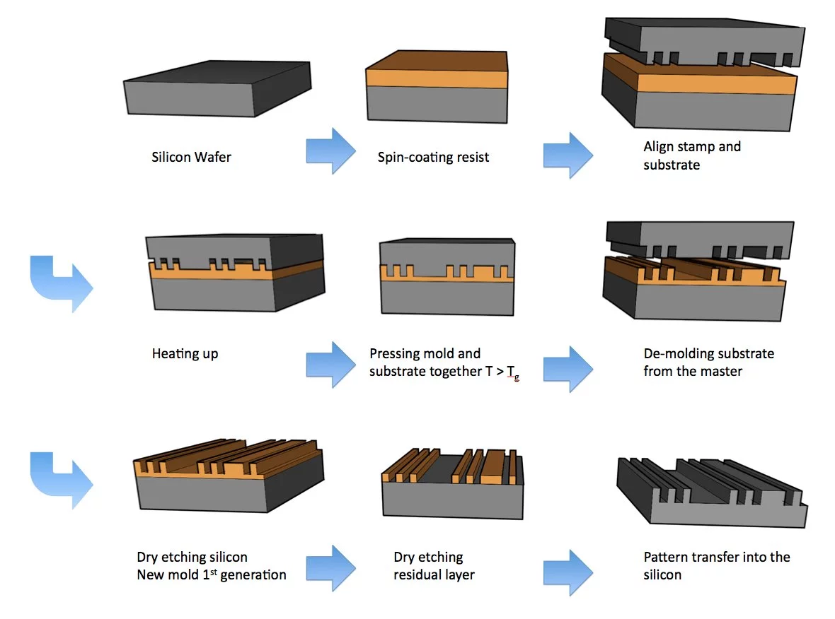
NIL Process Chain
NIL Process Chain
The process chain mainly consists of the three steps:
  1. Align substrate, resist and stamp
  2. Imprint into polymer film
  3. Pattern transfer into substrate


The pattern transfer is often necessary if the imprinted polymer is not directly used as a functional material, but for patterning a large area substrate such as a silicon wafer or magnetic disc. It is therefore able to replace common high resolution lithography which is either costly or not able to pattern complex structures with 3D surface topographies.

Publications

Nanoimprint lithography: An old story in modern times? A review
J. Vac. Sci. Technol. B 26(2), 458-480 (2008)
Helmut Schift

NaPa Library of Processes
editor H.Schift, published by the NaPa-consortium
first edition (2008) ISBN 978-3-00-024396-7, second edition (2012)
Free download: NaPa Library of Processes

Nanoimprint lithography - patterning resists using molding
H. Schift and A. Kristensen
Handbook of Nanotechnology, Chapter (Part A/9), third edition, revised and extended, 2010
Springer Verlag Berlin Heidelberg, Germany. ISBN: 978-3-642-02524-2

Sidebar

Contact

Dr. Helmut Schift

Laboratory for Micro-
and Nanotechnology
Paul Scherrer Institut
5232 Villigen PSI
Switzerland

Telephone: +41 56 310 2839
E-mail: helmut.schift@psi.ch

top

Pied de page

Paul Scherrer Institut

Forschungsstrasse 111
5232 Villigen PSI
Suisse

Téléphone: +41 56 310 21 11
Téléfax: +41 56 310 21 99

Comment nous trouver 
Contact

Centre de visiteurs psi forum
Laboratoire élèves iLab (en allemand)
Centre de protonthérapie
Centre de Formation du PSI
PSI Guest House (en anglais)
PSI Gastronomie (en allemand)
psi forum shop

Service & Support

  • Annuaire
  • User Office
  • Accelerator Status
  • Publications du PSI
  • Fournisseurs
  • E-facture
  • Computing (en anglais)
  • Sicherheit (en allemand)

Carrière

  • Travailler au PSI
  • Offres d'emploi
  • Formation initiale et formation continue
  • Career Center
  • Formation professionnelle (en allemand)
  • Centre de Formation du PSI

Pour les médias

  • Le PSI en bref
  • Chiffres et faits
  • Le coin médias
  • Communiqués de presse
  • Réseaux sociaux

Suivez le PSI: Twitter (in English) LinkedIn Youtube Facebook Instagram Issuu RSS

Footer legal

  • Impressum
  • Conditions d'utilisation
  • Login éditeurs