The work in IPN has a strong focus on semiconductor technology development and developing novel device architectures for electronics and photonic components. In addition, we enjoy exploring different characterization techniques to get a better understanding of the device physics. To this end, we collaborate with a number of excellent researchers internationally.
The work in INPHO has a strong focus on semiconductor technology development and developing novel device architectures for electronics and photonic components. In addition, we enjoy exploring different characterization techniques to get a better understanding of the device physics. To this end, we collaborate with a number of excellent researchers internationally.
Some examples of research projects which were carried out at IBM Research Europe Zurich are shown below. New projects are being shaped at PSI along the same themes.
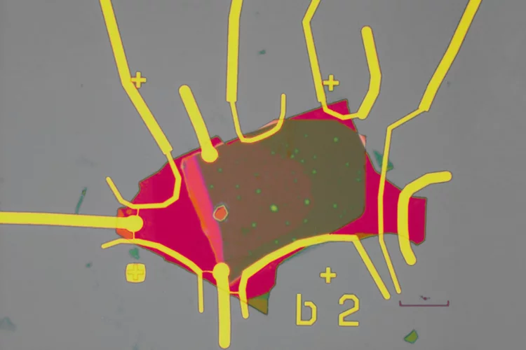

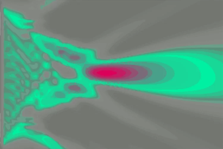

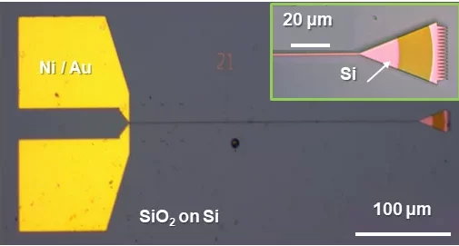
Nanostructured materials-based noise reduction and field enhancement of optomechanical nano resonators for quantum cavity optomechanics
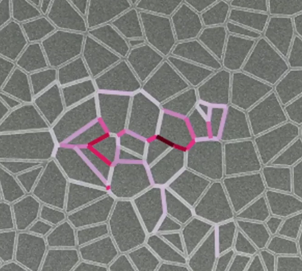
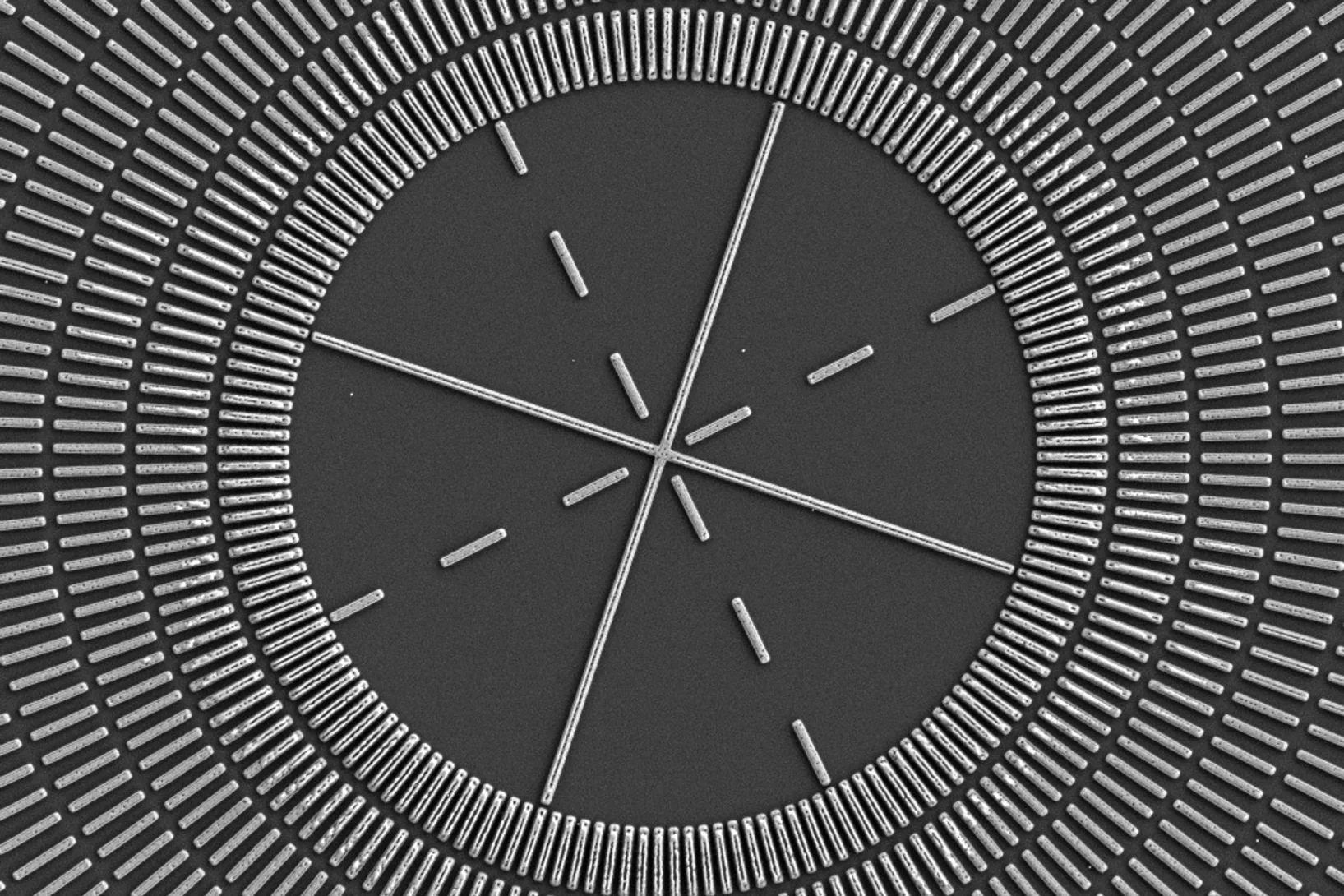
NEON : Neuromorphic photonics and III-V Electro-Optic modulators for random lasing Networks
The goals of the NEON project are a deeper scientific understanding of the physics of neuromorphic photonic networks, an improved architecture, and finally a path towards higher energy efficiency. The researchers hope to achieve and demonstrate a fully integrated neuromorphic photonic platform with a diameter of only around 100 micrometres.
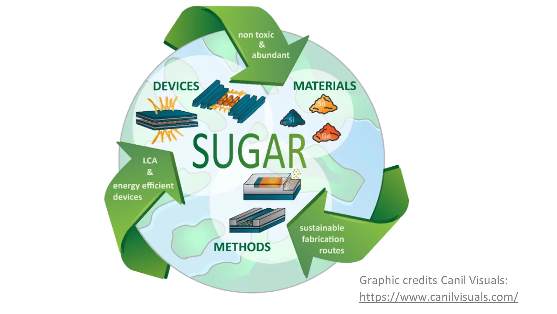
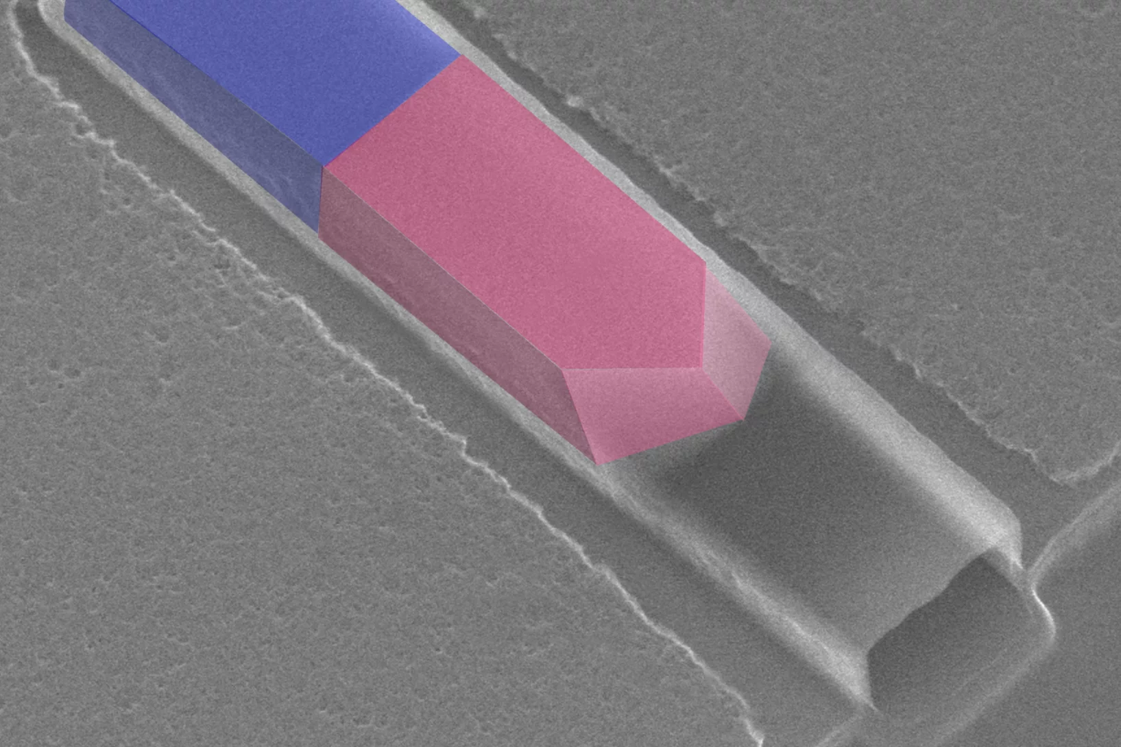
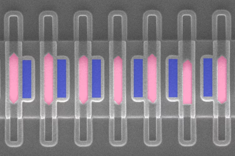
SUGAR : Sustainable Group-IV Active Photonics Research
The SUGAR project aims to develop a more sustainable photonics platform, focusing on group IV elements (Si, Ge, Sn) that are non-toxic and abundant. The proposal emphasizes sustainability throughout the entire device life-cycle, incorporating life-cycle analysis (LCA) from extraction to end-of-life.