Aller au contenu principal
  • Paul Scherrer Institut PSI
  • PSI Research, Labs & User Services

Digital User Office

  • Digital User Office
  • DE
  • EN
  • FR
Paul Scherrer Institut (PSI)
Rechercher
Paul Scherrer Institut (PSI)

Hauptnavigation

  • Research at PSIOuvrir ce point de menu principal
    • Research Initiatives
    • Research Integrity
    • Scientific Highlights
    • Scientific Events
    • Scientific Career
    • PSI-FELLOW
    • PSI Data Policy
  • Research Divisions and LabsOuvrir ce point de menu principal
    • Overview
    • Research with Neutrons and Muons
    • Photon Science
    • Energy and Environment
    • Nuclear Energy and Safety
    • Biology and Chemistry
    • Large Research Facilities
  • Facilities and InstrumentsOuvrir ce point de menu principal
    • Overview
    • Large Research Facilities
    • Facilities
    • PSI Facility Newsletter
  • PSI User ServicesOuvrir ce point de menu principal
    • User Office
    • Methods at the PSI User Facilities
    • Proposals for beam time
    • Proposal Deadlines
    • Data Analysis Service (PSD)
    • EU support programmes
  • DE
  • EN
  • FR

Digital User Office (mobile)

  • Digital User Office

Vous êtes ici:

  1. PSI Home
  2. Labs & User Services
  3. PSD
  4. LMN
  5. Research Groups
  6. Molecular Nanoscience
  7. SiC: Surfaces and Interfaces

Navigation secondaire

Laboratory for Micro and Nanotechnology

  • About LMN
    • Organisational Structure
  • Open Positions
  • People
  • Research Groups Sous-menu élargi
    • Nanotechnology
    • X-ray Optics and Applications
      • X-ray Optics for Imaging and Spectroscopy
        • Fresnel Zone Plate for X-ray Microscopy
        • Blazed X-ray Optics
        • Zernike X-ray Phase Contrast Microscopy
        • Fresnel Zone Plates for RIXS
        • Refractive Lenses by 2 Photon 3D Lithography
      • Wavefront Metrology and Manipulation
        • Vortex Fresnel Zone Plates
        • Grating-based Wavefront Metrology
      • X-ray Optics for XFELs
        • Diamond Fresnel Zone Plates
        • Beam Splitter Gratings for Spectral Monitoring
        • A Delay Line for Ultrafast Pump-Probe Experiments
        • X-ray Streaking for Ultrafast Processes
    • Polymer Nanotechnology
      • Nanoimprint Lithography
      • Three Dimensional Structures
    • Molecular Nanoscience Sous-menu élargi
      • On-surface Chemistry
      • Spins in Molecular Monolayers
      • SiC: Surfaces and Interfaces
      • Our Research Team
    • Advanced Lithography and Metrology
      • EUV Interference Lithography
      • EUV Lensless Imaging
      • ALM Nanoscience
    • Quantum Technologies
      • News and highlights
      • People
      • Open positions
      • Current projects
        • 2D semiconductor devices
        • CDW-based memory devices
        • Imaging quantum many-body states
        • Nonlinear magnonics
        • Rare-earth quantum magnets
        • Strained Germanium laser
      • Techniques
        • Cristallina-Q
        • IR beamline
        • Nano-fabrication
      • Publications
      • QTC@PSI
  • Facilities and Equipment
    • Cleanroom Labs
    • Surface Science Lab
    • Scanning Electron Microscopy
    • Scanning Probe Microscopy
    • PEARL Beamline
    • XIL Facility at the SLS
    • Nanoimprint Facilities
    • Electron Beam Lithography
  • LMN News
  • LMN Highlights
    • Archive
  • Publications
    • Publications 2011 - 2016

Info message

Ce contenu n'est pas disponible en français.

SiC: Power devices, Interfaces and their Characterization

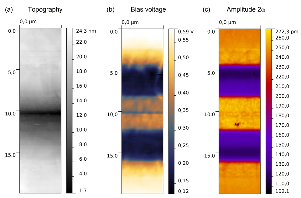
Fig. 1. Simultaneously acquired topographic image (a) while KPFM (b) and 2ω EFM (c) measurements were performed by the oscillation of the second eigenmode. To avoid rounding effects at the sample edges two samples were glued together with non-conductive epoxy.

For power semiconductor devices the two main figures of merit are (i) a high blocking voltage capability, which minimizes the re‐ verse current in the OFF‐state and (ii) a low ON‐state resistance when the device is operated under forward conditions. The mate‐ rial properties of silicon carbide are expected to be superior to sili‐ con because of their higher critical electric field and higher thermal conductivity. This properties can be integrated into devices like Schottky diodes, MOS capacitors and planar MOSFETs. Thereby higher switching speeds can be achieved at lower power dissipa‐ tion. A significant challenge and current limitation in performances of active devices is due to the low channel mobilities inside the in‐ version channel at the 4H‐SiC/insulator interface and the increas‐ ing junction‐FET resistance causing the downscaling of these de‐ vices. Various interface passivation treatments therefore have been tested which resulted in a slight mobility improvement of current devices. However the ob‐ tained mobilities are still far below the theoretical bulk value and the physical origin of the mobility enhancing mechanism still remains unclear.

Current research activities:

  • Atomic‐Scale Analysis of SiC‐Oxide Interface for Improved High‐Power MOSFETs [1]
  • Wide Band Gap Power Semiconductors Improved by Nanoscale Probe Analytics [2]
  • Physical Studies of SiC Nano‐Trench‐MOSFETs [3]

Publications

[1] Evidence for carbon clusters present near thermal gate oxides affecting the electronic band structure in SiC-MOSFET.
D. Dutta et al.
Editor’s Pick in Appl. Phys. Lett. 115, 101601 (2019);


[2] Improving the Design of the Shield for the Electric Field in SiC-Based Schottky-Rectifiers and Ion-Implantation Cascades by SPM Dopant-Imaging.
H. Rossmann et al.
Microelectronic Engineering 148 (2015) 1–4


[3] Device Simulations on Novel High Channel Mobility 4H-SiC Trench MOSFETs and Their Fabrication Processes
H. R. Rossmann, A. Bubendorf, F. Zanella, N. Marjanović, et al.
Microelectron. Eng. 145, 166 (2015)

Sidebar

Contact

Prof. Thomas Jung

Laboratory for Micro-
and Nanotechnology
Paul Scherrer Institut
5232 Villigen PSI
Switzerland

Telephone:
+41 56 310 4518
Telefax:
+41 56 310 2646
E-mail:
thomas.jung@psi.ch

top

Pied de page

Paul Scherrer Institut

Forschungsstrasse 111
5232 Villigen PSI
Suisse

Téléphone: +41 56 310 21 11
Téléfax: +41 56 310 21 99

Comment nous trouver 
Formulaire de contact

Centre de visiteurs psi forum
Laboratoire élèves iLab (en allemand)
Centre de protonthérapie
Centre de Formation du PSI (en allemand)
PSI Guest House (en anglais)
PSI Gastronomie (en allemand)

Service & Support

  • ​Annuaire/Liste de contacts
  • User Office
  • Accelerator Status
  • Publications du PSI
  • Fournisseurs
  • E-facture
  • Computing (en anglais)
  • Sicherheit (en allemand)

Carrière

  • Travailler au PSI
  • Offres d'emploi
  • Formation initiale et formation continue
  • Formation professionnelle (en allemand)
  • Centre de Formation du PSI

Pour les médias

  • Le PSI en bref
  • Chiffres et faits
  • Contact destiné aux médias
  • Communiqués de presse
  • Social Media Newsroom

Suivez le PSI: Twitter (en allemand) LinkedIn Youtube Issuu RSS

Footer legal

  • Impressum
  • Conditions d'utilisation
  • Login éditeurs