Aller au contenu principal
  • DE
  • EN
  • FR
Paul Scherrer Institut (PSI) Paul Scherrer Institut (PSI)
Rechercher
Paul Scherrer Institut (PSI) Paul Scherrer Institut (PSI)

Hauptnavigation

  • Labs & User ServicesOuvrir ce point de menu principal
    • Overview
    • Research at PSI
    • Research Divisions and Labs
    • Facilities and Instruments
    • Research Initiatives
    • PSI User Labs
    • Scientific Highlights
    • Scientific Events
    • Scientific Career
    • Useroffice
  • VisiteursOuvrir ce point de menu principal
    • Aperçu
    • Contact
    • Comment nous trouver
    • Manifestations
    • Centre de visiteurs psi forum
    • Schülerlabor iLab
    • Centre de protonthérapie
  • IndustrieOuvrir ce point de menu principal
    • Aperçu
    • Le transfert de technologie
    • Entreprises spin-off
    • PARK innovAARE
  • Notre rechercheOuvrir ce point de menu principal
    • Actualités de notre recherche
    • Matière et matériaux
    • L'Homme et la santé
    • Energie et environnement
    • Grands instruments de recherche
    • Brochures Générales
    • Films
    • Pour les médias
  • Carrière & FormationOuvrir ce point de menu principal
    • Offres d'emploi
    • Politique du personnel
    • Travailler au PSI
    • Formation initiale et formation continue
    • Formation professionnelle
    • Centre de Formation du PSI
    • Programme de soutien "PSI Career Return Program"
    • PSI-FELLOW/COFUND
  • Sur le PSIOuvrir ce point de menu principal
    • Le PSI en bref
    • Stratégie
    • Chartes
    • Chiffres et faits
    • Organisation
    • Fournisseurs
    • Clients – e-facture
    • Infrastructure informatique (en allemand et en anglais)
    • Sécurité au PSI (en allemand)

Vous êtes ici:

  1. PSI Home
  2. Labs & User Services
  3. PSD
  4. LMN
  5. Research / Groups
  6. SwissFEL nanoengineering
  7. Vacuum Nanoelectronics
  8. Nanotip fabrication

Navigation secondaire

Laboratory for Micro and Nanotechnology

  • About LMN
    • Organisational Structure
  • People
  • Research / Groups Sous-menu élargi
    • X-ray Optics
      • Diffractive X-ray Lenses
        • Electroplated Zone Plates and Beam Shapers
        • Ultra-high Resolution Zone Plates
        • Double-Sided Zone Plates
        • Blazed X-ray Optics
        • Zernike X-ray Phase Contrast Microscopy
      • Grating-based X-ray Interferometry
        • Differential Phase Contrast and Dark-Field Imaging
        • Metrology Applications at Synchrotrons and XFELs
        • Grating Fabrication
      • Diamond X-ray Optics for XFEL Experiments
        • Diamond Zone Plates for XFELs
        • Beam Splitter Gratings for Spectral Monitoring
        • Ultra-Fast Pump-Probe Experiments
    • Polymer Nanotechnology
      • Nanoimprint Lithography
      • Three Dimensional Structures
      • Polymer Grafting
    • SwissFEL nanoengineering Sous-menu élargi
      • Protein Crystallography Using Ultrasonic Acoustic Levitation
      • Supports for Serial Protein Crystallography
        • SwissMX supports
      • Coherent Electron Wavefront Engineering
      • Bio-Interfaces
      • Vacuum Nanoelectronics Sous-menu élargi
        • Research in Field Emitter Arrays
        • Nanotip fabrication
        • Laser induced emission
        • Double gated FEAs
        • Picosecond switching
        • Emittance measurements
        • Uniformity control
    • Molecular Nanoscience
      • On-surface Chemistry
      • Spins in Molecular Monolayers
      • SiC: Surfaces and Interfaces
      • Our Research Team
    • Advanced Lithography and Metrology
      • EUV Interference Lithography
      • EUV Lensless Imaging
      • ALM Nanoscience
    • Quantum Technologies
      • News and Highlights
      • Open Positions
      • Group IV Photonics
      • Silicon Carbide Electronics
      • Optical Properties of Semiconductor Nanostructures
      • THz Plasmonics
      • QT People
      • QT Collaboration
  • Facilities and Equipment
    • Cleanroom Labs
    • Surface Science Lab
    • Chemistry Lab
    • Electron Beam Lithography
    • Nanoimprint Facilities
    • XIL Facility at the SLS
    • Scanning Probe Microscopy
    • Scanning Electron Microscopy
  • Meetings and Seminars
  • LMN News and Highlights
    • Archive
  • Publications
    • Publications 2011 - 2016

Info message

Ce contenu n'est pas disponible en français.

Fabrication of metallic field emitter array cathode

PSI field-emitter array cathode: overview
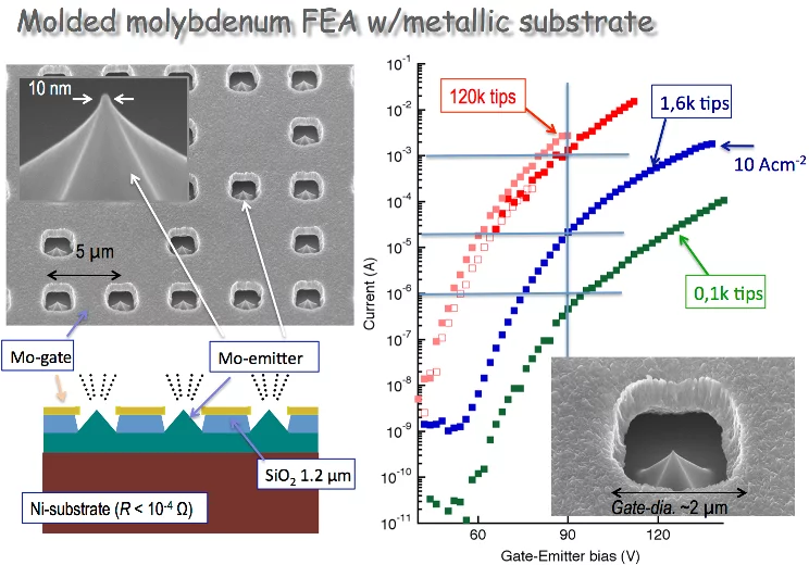
Unlike the celebrated Spindt FEA, first demonstrated by C.A. Spindt [1], the PSI all-metallic FEA fabrication method is based on a unique molding method [2,3] that can produce a uniform emitter-tip array over a large area. These metallic nanotips have tip apex radii of curvature in the order of a few nanometres. Single-gate and double-gate FEAs are fabricated based on the molded metallic field emitter arrays [2,3,4,5]. Development of sub-micron pitch FEAs to further increase the quantum efficiency of the laser-induced field emission is under way [6,7].


Array fabrication by molding

(a) directional etching of pyramidal pits into Si wafer
(b) multiple thermal oxidation steps control pit apex diameter
(c) sputter-fill mold with Molybdenum
(d) chemically remove Si wafer


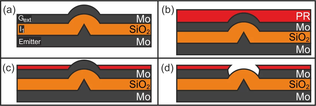
Gate fabrication: electron extraction electrode

(a) deposit insulator and extraction gate electrode
(b) spin-coat photoresist (PR)
(c) thin PR in oxygen plasma to form extraction gate aperture etch mask
(d) wet-etch Molybdenum


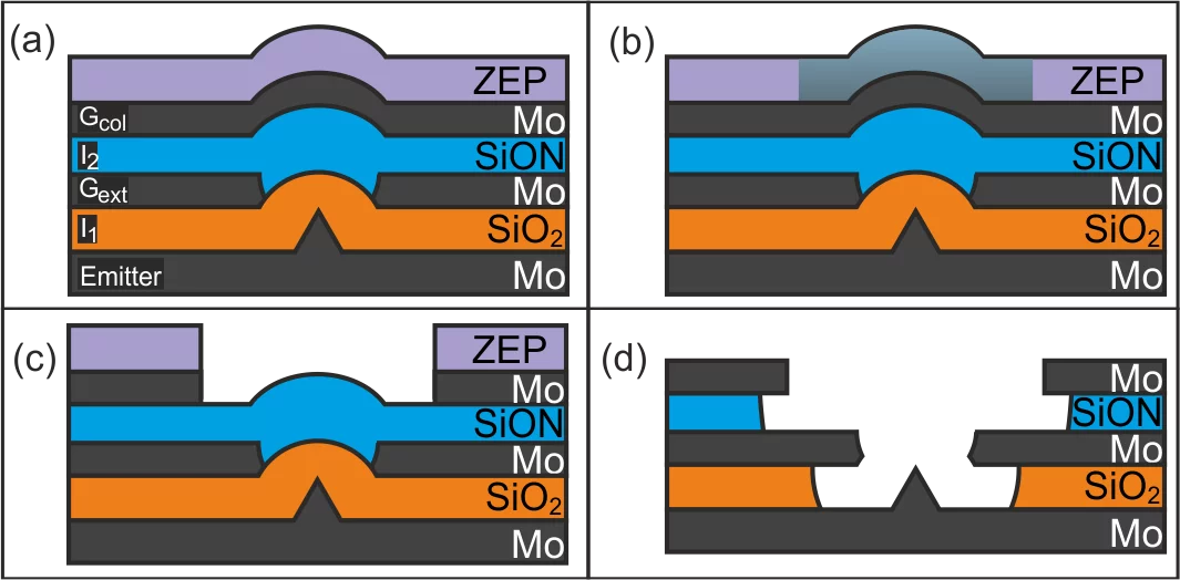
Gate fabrication: electron collimation electrode


(a) deposit insulator (SiON), collimation gate electrode and ZEP resist
(b) form collimation gate aperture by selectively exposing ZEP by e-beam lithography
(c) develop ZEP and wet-etch Molybdenum
(d) remove insulator on top of tips by wet-etching


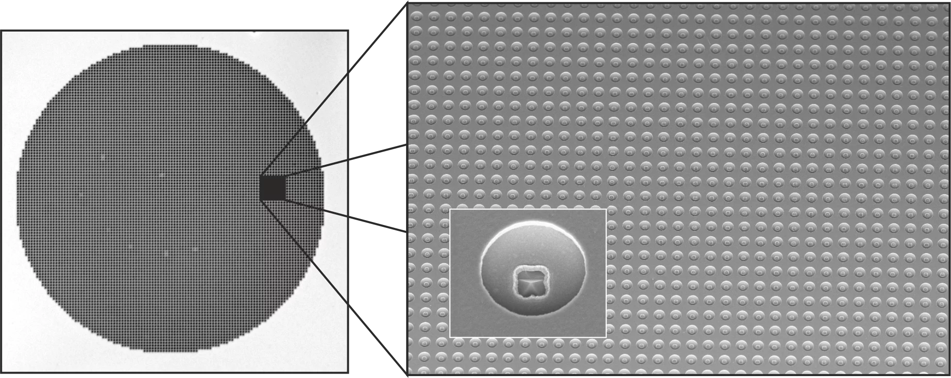
SEM images of the PSI-FEA

References

[1] C.A. Spindt, J. Appl. Phys. 39 3504 (1968).

[2] E. Kirk, S. Tsujino, T. Vogel, K. Jefimovs, J. Gobrecht, A. Wrulich, Fabrication of all-metal field emitter arrays with controlled apex sizes by molding, J. Vac. Sci. Technol. B 27, 1813 (2009).

[3] P. Helfenstein, E. Kirk, K. Jefimovs, T. Vogel, C. Escher, H.-W. Fink, and S. Tsujino, Highly collimated electron beams from double-gate field emitter arrays with large collimation gate apertures, Appl. Phys. Lett. 98, 061502 (2011).

[4] P. Helfenstein, K. Jefimovs, E. Kirk, C. Escher, H.-W. Fink, and S. Tsujino, Fabrication of metallic double-gate field emitter arrays and their electron beam collimation characteristics, J. Appl. Phys. 112, 093307 (2012).

[5] P. Helfenstein, V. A. Guzenko, H.-W. Fink, and S. Tsujino, Electron beam collimation with 40,000 tip metallic double gate field emitter arrays and in-situ control of nanotip sharpness distribution, J. Appl. Phys. 113, 043306 (2013).

[6] A. Mustonen, V. Guzenko, C. Spreu, T. Feurer, and S. Tsujino, High-density metallic nano-emitter arrays and their field emission characteristics, Nanotechnology 25, 085203 (2014).

[7] V. Guzenko, A. Mustonen, P. Helfenstein, E. Kirk, and S. Tsujino, High-density large-scale field emitter arrays for X-ray free electron laser cathodes, Microelectronic Engineering (2013).


Sidebar

Contact

Dr. Soichiro Tsujino

Laboratory for Micro-
and Nanotechnology
Paul Scherrer Institut
5232 Villigen PSI
Switzerland

Telephone:
+41 56 310 2304
Telefax:
+41 56 310 2646
E-mail:
soichiro.tsujino@psi.ch

IVNC2019

The 32th International Vacuum Nanoelectronics Conference (IVNC 2019) & 12th International Vacuum Electron Sources Conference (IVESC), 22-16, July 2019, in Cincinnati, Ohio, Japan.
top

Pied de page

Paul Scherrer Institut

Forschungsstrasse 111
5232 Villigen PSI
Suisse
Comment nous trouver 

Impressum 
Conditions d'utilisation

Login

Téléphone: +41 56 310 21 11
Téléfax: +41 56 310 21 99
Formulaire de contact 

Centre de visiteurs psi forum
Laboratoire élèves iLab (en allemand)
Centre de protonthérapie

Suivez le PSI: Twitter (en allemand) LinkedIn Youtube Issuu RSS

Quicklinks

  • Liste de contacts/​Annuaire
  • Digital User Office
  • Transfert de technologie
  • Publications du PSI
  • Computing (en anglais)
  • Sicherheit (en allemand)
  • Offres d'emploi
  • Berufsbildung (en allemand)
  • Fournisseurs
  • Clients – e-facture
  • PSI Guesthouse (en anglais)
  • PSI Gastronomie (en allemand)

Pour les médias

  • Contact destiné aux médias
  • Communiqués de presse
  • Social Media Newsroom
  • Chiffres et faits
  • Le PSI en bref
  • Films
  • DE
  • EN
  • FR