The conducting interface between LaAlO3 and SrTiO3
The physical mechanisms behind the unexpected formation of an ultrathin conducting layer at the interface between the band insulators SrTiO3 (STO) and LaAlO3 (LAO) have been the subject of considerable controversy since its discovery in 2004. Both STO and LAO belong to a technologically important family of materials called perovskites. In many of these materials, very small movements in the positions of the constituent atoms can have profound effects on their electronic properties, due mainly to the fact that the electrons involved in the bonds are strongly influenced by one another.
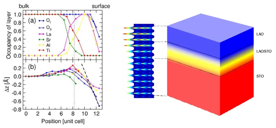
In the case of the LAO/STO interface, the situation is further complicated by the fact that LAO consists of a stacking of alternating oppositely charged sheets (LaO+ and AlO2-), while STO contains neutral layers. This causes an electric field to form at the interface, which can be neutralized either by the rearrangement of electrons (i.e., a local change in valence of the ions), or by the rearrangement or removal of atoms. Exactly which mechanisms play the most important role is the essence of the controversy. A common conclusion of the investigations to date is that the mechanisms will be better understood if a comprehensive description of the interface with sub-Angstrom resolution is made available. Surface x-ray diffraction (SXRD) is ideally suited for this. Using the Pilatus detector, a large SXRD data set of a 5-monolayer film of LAO grown on STO was recorded, and analyzed with phase-retrieval methods and subsequent structural refinement techniques. It was found that the interface between STO and LAO was not abrupt, but formed a graded layer of approximately 3 unit-cell thickness (see Figure). Importantly, this layer contains a significant fraction of Ti3+, which is incorporated into La1-xSrxTiO3 (LSTO), a conducting material in bulk form. Indeed, in this interfacial layer, LSTO is forced to assume a tetragonal structure (it is orthorhombic in the bulk), which should further enhance its conductivity. In this manner, the formation of the conducting layer has been explained based only on simple structural considerations. The electronic properties of this model were also investigated using a theoretical (density functional theory) calcuations, which confirmed the experimental findings.
See also: P.R. Willmott, S.A. Pauli, R. Herger, C.M. Schlepuetz, D. Martoccia, B.D. Patterson, B. Delley, R. Clarke, D. Kumah, C. Cionca, and Y. Yacoby, Phys. Rev. Lett 99, 155502 (2007)
doi:10.1103/PhysRevLett.99.155502
The surface of strontium titanate
Strontium titanate (SrTiO3, STO), a perovskite structure, is the most commonly used substrate material for the growth of thin films of complex metal oxides, such as high-temperature cuprate superconductors, colossal magnetoresistive materials, and ferroelectrics.
Despite the known influence that the surface structures of substrate materials have on nucleation processes and growth modes, there seems little agreement on the surface structure of STO.
Here we studied, using surface diffraction, the surface of STO(100), both after preparing the surface using a well-established wet-etch/annealing procedure, and subsequently under typical conditions for thin film growth, i.e., at 700oC and at 0.04 Pa O2.
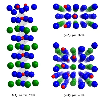
The etched surface was shown to consist of three different domain types, namely an approximately equal mixture of (2x1) and (2x2) reconstructions, plus a minor contribution from a (1x1) relaxation. The reconstructions have two characteristic features - first, the two uppermost atomic layers are not SrO and TiO, as found in bulk STO, but a double TiO-layer. Secondly, the titanium atoms in the topmost TiO layer describe a "zigzag" motif. Upon heating, the reconstructions disappeared over several minutes, leaving only the (1x1) relaxation.
The surface of SrTiO3(100): After etching in HF and annealing in O2, the surface consists of three domain types: a (1x1) relaxation, and a (2x1) and (2x2) reconstruction. All the domains exhibit a double TiO2 topmost layer and a "zigzag" motif of the Ti-atoms. Color code: Red = Ti; blue = O; green = Sr.
The surface of SrTiO3(100): After etching in HF and annealing in O2, the surface consists of three domain types: a (1x1) relaxation, and a (2x1) and (2x2) reconstruction. All the domains exhibit a double TiO2 topmost layer and a "zigzag" motif of the Ti-atoms. Color code: Red = Ti; blue = O; green = Sr.
See also: R. Herger, P.R. Willmott, O. Bunk, C.M. Schlepuetz, B.D. Patterson, and B. Delley, Phys. Rev. Lett 98, 076102 (2007)
doi:10.1103/PhysRevLett.98.076102
Kinetic studies of monolayer growth in pulsed laser deposition
An epitaxial growth method which deserves special mention is pulsed laser deposition (PLD). It is a nonthermal technique capable of producing stoichiometric films containing many atomic species, without the need of dangerous metallorganic precursors. The one unique property of PLD is the magnitude of the transient deposition flux of the laser-ablated species, which is orders of magnitude higher than in any other deposition technique. This leads to novel growth modes in thin film deposition by causing film formation to be seeded by a high areal density of very small nucleation sites.
One aspect of growing thin films of novel materials, is that smooth surfaces are a must. How else could one stack them layer by layer, as needed in optical coatings, sensors or conductors? With every pulse of deposition flux in PLD, a jet (or “plume”) of high energy atoms is created. When these condense on a smooth substrate, they recreate the target material, but now as a thin film. Per laser pulse only about 1/100th of an atomic layer is deposited on the substrate.
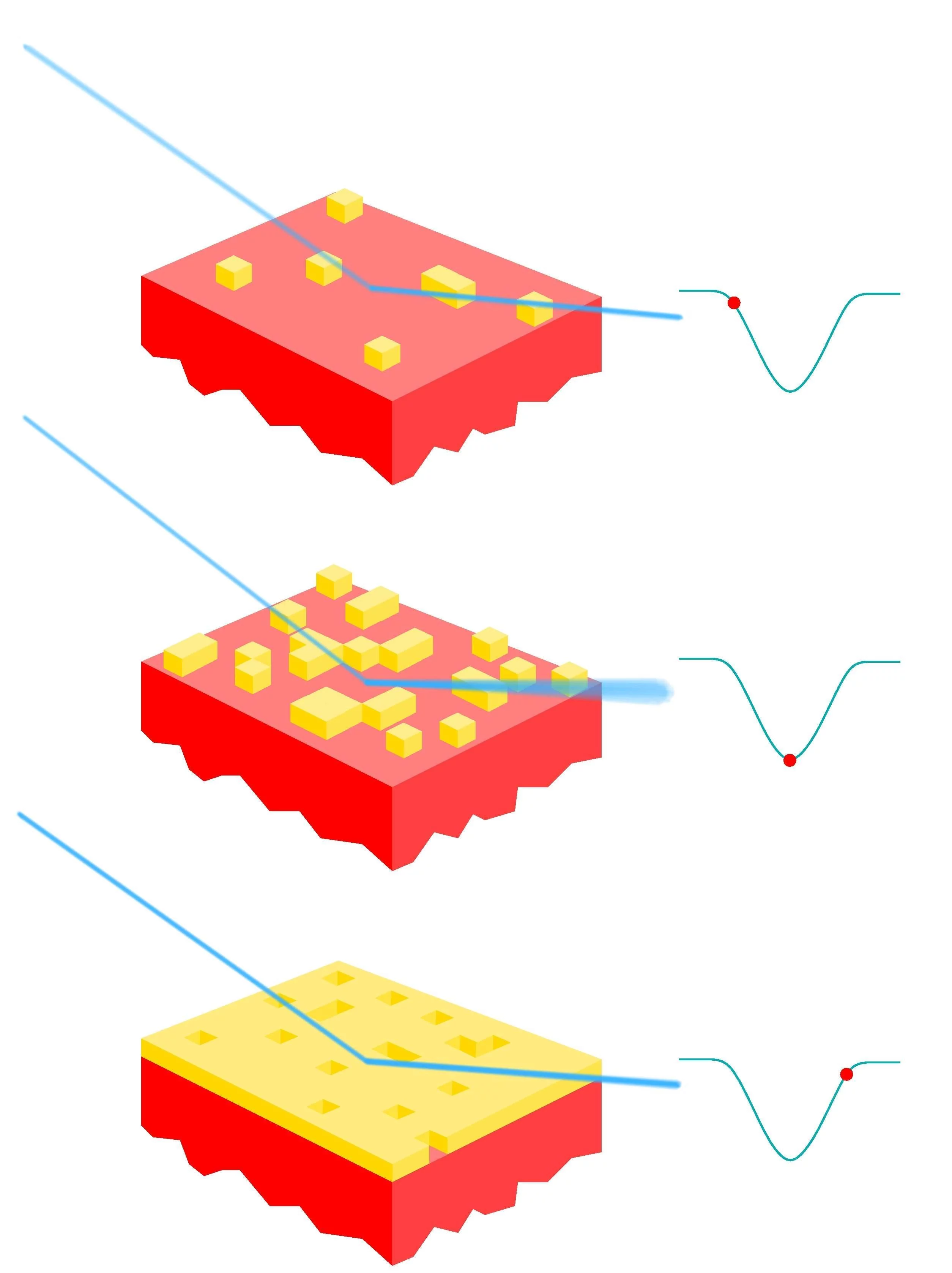
Although the fact that PLD produces atomically smooth films has long been known, the reasons for this were somewhat speculative. A recent experiment at the SD station, using an in-situ PLD chamber, measured the roughness of PLD films, carefully adding one laser pulse after another. This provided the clue to the puzzle: when the first atoms land on the smooth substrate they form small islands of the material. Subsequent pulses lead either to formation of more small islands if the particles land on an uncovered part of the monolayer, or, importantly, cause already formed islands to break up if the energetic particles land on top of them. This avoids growth of "islands on top of islands", which would gradually result in rough films. Now that the process is understood, one can optimally tune PLD for growing thin films of materials which are then used in devices. See also article DOI: 10.1103/PhysRevLett.96.176102
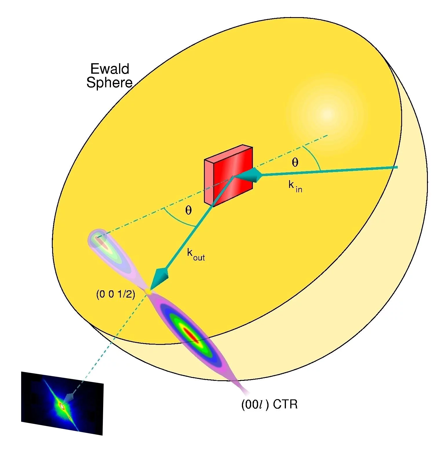
X-ray reflectivity measurements: The specularly reflected x-rays are monitored exactly in between Bragg maxima [here, at the (0 0 1/2) position], where the sensitivity to changes in the surface morphology is highest. The signal becomes weakest when the roughness is maximal, i.e., when half a monolayer is deposited
See also: P.R. Willmott, R. Herger, C.M. Schlepuetz, D. Martoccia, and B.D. Patterson, Phys. Rev. Lett 96, 176102 (2006)
doi:10.1103/PhysRevLett.96.176102
P.R.W. February 2007


