Show filters
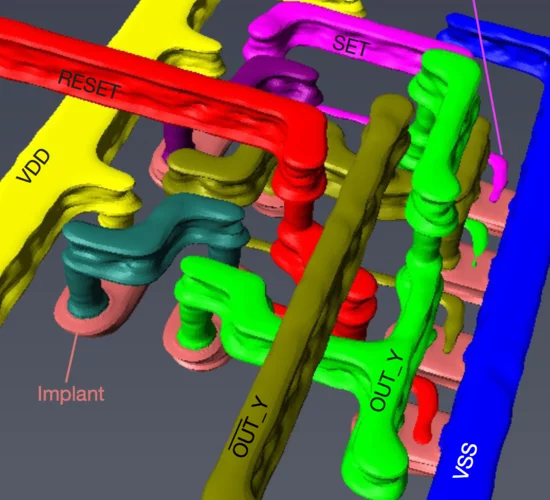
High-resolution non-destructive three-dimensional imaging of integrated circuits
Modern nanoelectronics has advanced to a point at which it is impossible to image entire devices and their interconnections non- destructively because of their small feature sizes and the complex three-dimensional structures resulting from their integration on a chip. This metrology gap implies a lack of direct feedback between design and manufacturing processes, and hampers quality control during production, shipment and use.
Search for the lepton flavour violating decay μ+→e+γ with the full dataset of the MEG experiment
The final results of the search for the lepton flavour violating decay μ+→e+γ based on the full dataset collected by the MEG experiment at the Paul Scherrer Institut in the period 2009–2013 and totalling 7.5×10¹⁴ stopped muons on target are presented.


