Coherent Electron Source
Field emitters produce high-brightness, highly coherent electron beams that underpin atomic-resolution electron microscopy. Beyond brightness, they can deliver high current density and narrow angular spread, which is why field emitters have been central to high-frequency vacuum electronics, accelerator injectors, and coherence-based experiments such as electron diffraction, holography, and coherent diffraction imaging.
A key open question is how spatial coherence at the cathode propagates. Field-emission electrons tunnel through the surface barrier, so the emitted wavefunction inherits the momentum distribution of electrons in the solid. This connection constrains the minimal transverse source size and the coherent fraction of the beam [1,2]. Our analyses indicate that beam propagation and transverse emittance are set by the average transverse energy (ATE) of field emission as given by standard theory [1–4]. Recent measurements on double-gate Mo nanotip FEAs [3] and single Mo nanotips with on-chip collimation [5] are consistent with this picture: the minimal beam spread at optimal collimation and the emittance scale with the ATE.
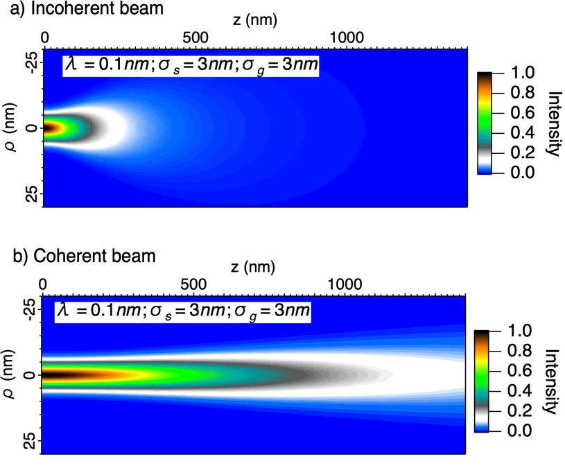
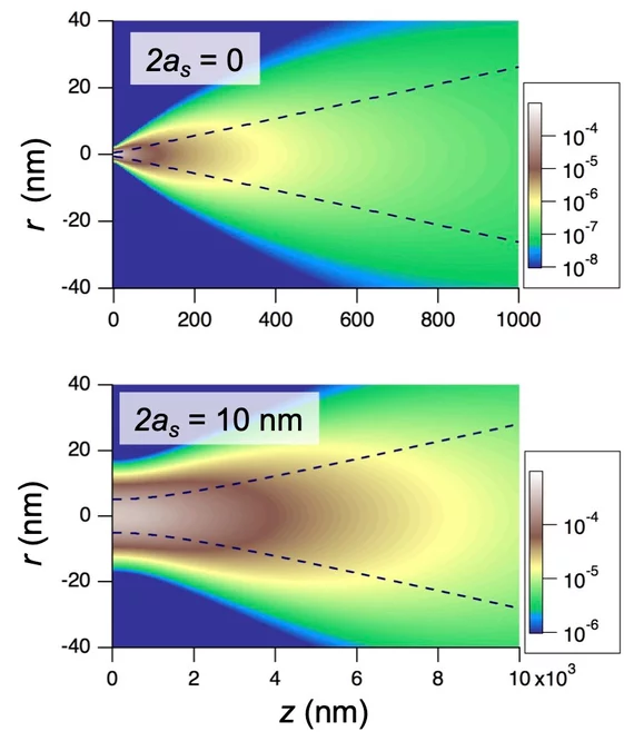
From [2], a single Mo nanotip with a 5–10 nm apex radius is expected to show a coherent fraction of ~10–20 %, based on a minimal source size of ~1 nm (uncertainty limit) and ATE ~0.1 eV. Treating propagation with the theory of partially coherent beams [5] (which predicts conservation of coherent fraction under free-space propagation), one obtains micron-scale spatial coherence without additional apertures—much larger than van Cittert–Zernike estimates (tens of nm) for an incoherent source. Current LEED-based coherence-length measurements [6] are not yet decisive between these models. Figure 1 illustrates how finite source coherence narrows the far-field beam envelope [2], and Figure 2 shows that a finite coherent source size further reduces beam spread in the fully coherent limit [1]. Because coherence governs algorithmic imaging (coherent scattering + computational reconstruction), this remains an active research area.
Referernces
[1] S. Tsujino, Transverse structure of the wave function of field emission electron beam determined by intrinsic transverse energy, J. Appl. Phys. 124, 044304 (2018). https://doi.org/10.1063/1.5035284,
[2] S. Tsujion, On the brightness, transverse emittance, and transverse coherence of field emission beam, Journal of Vacuum Science & Technology B 40, 030801 (2022) (featured article); https://doi.org/10.1116/6.0001776.
[3] S. Tsujino, P. D. Kanungo, M. Monshipouri, C. Lee, and R. J. D. Miller, Measurement of transverse emittance and coherence of double-gate field emitter array cathodes, Nat. Commun. 7, 13976 (2016); https://doi.org/10.1038/ncomms13976.
[4] CR. H. Good and E. W. Müller, “Field emission,” in Electron-Emission Gas Discharges I/Elektronen-Emission Gasentladungen I (Springer, Berlin, 1956), pp. 176–231.
[5] C. Lee, P. D. Kanungo, V. A. Guzenko, P. Hefenstein, R. J. D. Miller, and S. Tsujino, Field emission beam characteristics of single metal nanotip cathodes with on-chip collimation gate electrode, J. Vac. Sci. Technol. B 33, 03C111 (2015);https://doi.org/10.1116/1.4913397.
[6] C. Lee, S. Tsujino, and R. J. D. Miller, Transmission low-energy electron diffraction using double-gated single nanotip field emitter, Appl. Phys. Lett. 113, 013505 (2018);https://doi.org/10.1063/1.5030889.
Electron wavefront engineering
Goal. Manipulate the phase and amplitude of coherent free-electron waves to enable new diffraction/imaging modalities. Unlike optics (where spatial light modulators synthesize arbitrary wavefronts), programmable electron-beam control is still limited. Notably, the textbook Young’s double-slit demonstration in Feynman’s lectures [7] was only directly realized with modern electron optics in the 2000s [8,9], though electron interference itself dates to the 1961 experiments of Jönsson [10].
Boersch Phase Shifters
A Boersch phase plate shifts the electron phase proportional to the applied potential, enabling in-situ, voltage-controlled phase modulation. Arrays of Boersch elements therefore offer a route to programmable electron wavefronts.
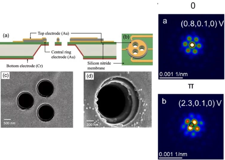
- Three-element device (fabrication + demo). In [11], we developed a CMOS-compatible electron-beam lithography + RIE process to fabricate three-element metal–insulator–metal (MIM) phase shifters with ~100 nm-thick ring electrodes and characterized them at 200 keV in a TEM. We observed voltage-controlled evolution of three-beam interference, demonstrating an electron phase shift on the order of π rad V⁻¹ (geometry-dependent), in agreement with 3-D electrostatic simulations.
- Five-layer shielding to suppress crosstalk. A follow-up MIMIM design (top/bottom shields) substantially reduced beam deflection and inter-element crosstalk, validating the scalability to larger arrays [12].
- Publication: high-energy interference control in JJAP.
Thakkar et al., Japanese Journal of Applied Physics 63, 104501 (2024), DOI 10.35848/1347-4065/ad7341: demonstrated electrostatic interference control of a high-energy (200 keV) coherent electron beam using three-element Boersch phase shifters built in an MIMIM stack, achieving minimal beam deflection and stable three-beam interference. This article consolidates the shielding strategy and verifies low-crosstalk, voltage-programmable phase control suitable for up-scaling to many elements.
Referernces
[7] R. P. Feynman, R. B. Leighton, M. Sands, The Feynman Lectures on Physics (Addition‐Wesley, Menlo Park, CA, 1965), Vol. III. III, Ch. 1, section 1‐5.
[8] S. Frabboni, G. C. Gazzadi, G. Pozzi, Young’s double‐slit interference experiment with electrons, Am. J. Phys. 75, 1053 (2007).
[9] R. Bach, D. Pope, S.‐H. Liou, H. Batelaan, Controlled double‐slit electron diffraction, New J. Physics 15, 033018 (2013).
[10] C. Joensson, Elektroneninterferenzen an mehreren kuenstlich hergestellten Feinspalten, Z. Physik 161, 454 (1961).
[11] P. Thakkar, V. A. Guzenko, P.-H. Lu, R. E. Dunin-Borkowski, J. P. Abrahams, S. Tsujino, Fabrication of low aspect ratio three-element Boersch phase shifters for voltage-controlled three electron beam interference, J. Appl. Phys. 128, 134502 (2020); https://doi.org/10.1063/5.0020383.
[12] P. Thakkar, V. A. Guzenko, P.-H. Lu, R. E. Dunin-Borkowski, J. P. Abrahams, S. Tsujino, Voltage-controlled three-electron-beam interference by a three-element Boersch phase shifter with top and bottom shielding electrodes, 34th International Vacuum Nanoelectronics Conference (Lyon, France, 2021); https://doi.org/10.1109/IVNC52431.2021.9600711.
[13] P. Thakkar, V. A. Guzenko, P.-H. Lu, R. E. Dunin-Borkowski, J. P. Abrahams, S. Tsujino, Electrostatic interference control of a high-energy coherent electron beam using three-element Boersch phase shifters, 2024 Jpn. J. Appl. Phys. 63 104501; DOI: 10.35848/1347-4065/ad7341


