Silicon Carbide is a wide bandgap semiconductor (3.2eV bandgap for the 4H polytype) with several Spin active photon emitters (SPEs) with optical transitions in the near-infrared and coherent electronic spins, including:
- VCVSi, named di-vacancy: Zero photon lines (ZPL) at 1079nm and 1131nm, lifetime of excited state of 14ns, coherence time of fundamental state of more than 1ms [1]. Demonstrate realization of isolated single defects. Demonstrated control through electric fields and mechanical strain [2].
- VSi, named Si-vacancy: Zero photon lines (ZPL) at 862nm and 917nm, lifetime of excited state of 5.3ns, coherence time of fundamental state of more than 1us [3]. Demonstrate realization of isolated single defects.
- Vanadium interstitials V4+ (3d1): Zero photon lines (ZPL) at 1278nm and 1334nm, lifetime of excited state of 160 and 40ns, coherence time of fundamental state of more than 100ns [4].
- Molybidenum interstitials Mo5+ (4d1): Zero photon lines (ZPL) at 1076nm, lifetime of excited state of 40ns, coherence time of fundamental state of more than 1us [4].
Di-vacancy and Si-vacancies have potential applications on quantum sensing and computation, with the foreseen possibility of long range spin-phonon coupling similarly with what is predicted for NV centers in diamond [5]. But, whereas studies on diamond require expensive special mm-sized samples, large SiC wafers with quality sufficient for quantum technology are already available. Also, in contrast to diamond, SiC is routinely p- and n-doped to make electronic devices. Selective etching, either on hetero-epitaxial structures (3C-SiC/Si) or by electro-chemistry in n-p doped regions, has been used to fabricate high-quality mechanical structures and optical microcavities. The available wealth of processing techniques will enable integrated devices containing electronics and quantum photonics. Furthermore, the electro-optic properties of SiC offer prospects towards the integration of active photonic components
V4+ and Mo5+ interstitials, on the other hand, have ZPL in the telecommunications “O”-band, thereby enabling extremely low-loss photon propagation. Furthermore, these two defects contain electronic and nuclear spins which can act as memories in quantum repeater nodes. This method would permit the creation of robust transcontinental quantum information links.
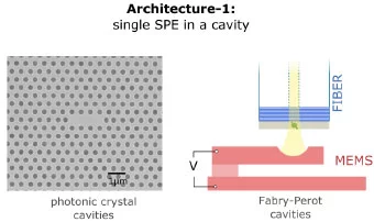
The Paul Scherrer Institute is currently engaged on the realization of micro-fabrications (photon-crystal and Fabry-Perot cavities) for the enhancement of the spin-photon interface properties of these defects.
[1] https://www.nature.com/articles/nmat4144
[2] https://journals.aps.org/prl/abstract/10.1103/PhysRevLett.112.187601
[3] https://www.nature.com/articles/nmat4145
[4] https://arxiv.org/abs/1802.06714
[5] http://dx.doi.org/10.1103/PhysRevLett.110.156402
Contact
Dr. Maria del Mar Carulla Areste
Laboratory for Micro and Nanotechnology
+41 56 310 3574
maria.carulla@psi.ch
