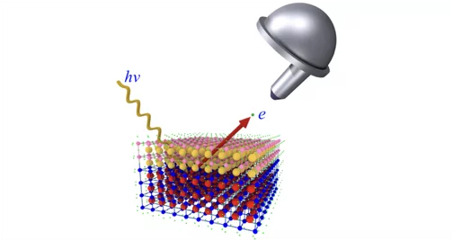
Buried heterostructure systems (interfaces and quantium wells of oxide compounds, semiconductors and topological materials) and impurity systems (magnetically doped semiconductors and topological materials) form the basis of many quantum devices. Fundamental electronic structure characteristics of these systems such as Fermi surface and band dispersions resolved in electron momentum k can be accessed with angle-resolved photoelectron spectroscopy (ARPES) using soft-X-ray synchrotron radiation with photon energy ~1 keV delivered by the ADvanced RESonant Spectroscopies (ADRESS) beamline of the Swiss Light Source. Enhancement of the photoelectron mean free path in this energy range allows access to buried interfaces and quantum wells, and chemical specificity achieved with resonant photoexcitation informs local electronic structure of magnetic and non-magnetic impurities. The current projects include oxide interfaces, semiconductor transistor heterostructures, magnetically doped semiconductors and topological materials, etc.
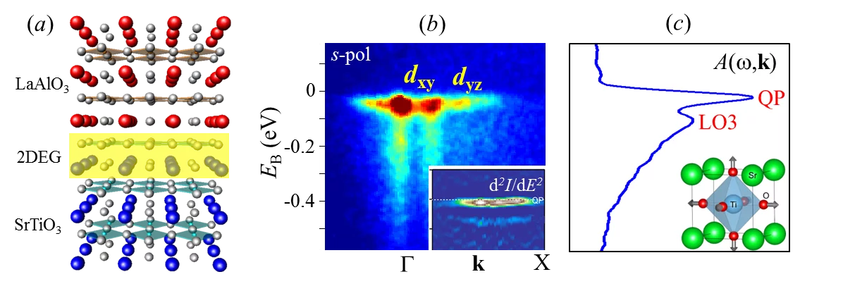
Oxide heterostructures. Interplay of spin, charge, orbital and lattice degrees of freedom in oxide heterostructures results in a plethora of fascinating properties, which can be exploited in new generations of electronic devices with enhanced functionalities. For example, superconducting Josephson junctions realized on the oxide platform are conceived as switching elements whose power consumption would reduce by 5 orders of magnitude compared to the current semiconductor electronics. A "drosophila" example of buried oxide interface is LaAlO3/SrTiO3 that embeds mobile 2D electron gas (2DEG) where co-existing are superconductivity and ferromagnetism. Resonant soft-X-ray ARPES resolves the multi-orbital Fermi surface and energy bands of electrons in the interface quantum well (QW). Their peak-dip-hump spectral lineshape manifests polaronic nature of the interface charge carriers that fundamentally limits their mobility [1]. A foe to mobility at higher temperature, the polaronic coupling may become its ally at low temperature by mediating formation of superconducting Cooper pairs. Doping of the LaAlO3/SrTiO3 interface with oxygen vacancies, affecting electron-phonon coupling, opens ways to tune the interfacial mobility. For more on oxide interfaces see the PSI media release. Other research cases on oxides include multiferroic BaTiO3/La1-xSrxMnO3interfaces, EuO/Si spin injectors, etc.
Semiconductor heterostructures. An example of buried semiconductor interfaces is an AlGaN/GaN high electron mobility transistor (HEMT) structure. Compared to the GaAs-based HEMTs, used in high-frequency circuits of every smartphone, these devices offer higher carrier density and power limit allowing their efficient use in microwave radars and radio tranmitters. Our soft-X-ray ARPES experiments establish the fundamental electronic structure characteristics of the quantized 2DEG buried in the conducting GaN channel, such as anisotropic Fermi surface, band dispersions and effective masses. Furthermore, the use of synchrotron radiation with tunable photon energy informs the wavefunction character of the 2DEG states. These spectroscopic findings suggest techological routes to further increase electron mobility and push the operational range of such transistor structures to yet higher frequencies. This application oriented research field is presently expanding to doped delta-layers, QWs and their superstructures building up artificial dimensionalities. The achieved fundamental knowledge helps engineering of semiconductor heterostructures with optimized device performance.
Magnetically doped semiconductors and topological materials. Tunable synchrotron radiation allows the use of resonant photoexcitation to explore local electronic structure of magnetic and non-magnetic dopants of transition and rear-earth metals with atomic concentration down to the promille level. One example is the paradigm diluted magnetic semiconductor (Ga,Mn)As where resonant soft-X-ray ARPES experiments identify the ferromagnetic Mn impurity band and establish its energy alignment and mechanism of hybridization with the host GaAs bands. Such studies lay down the fundamental physics of diluted magnetic semiconductors tailored to their applications in spintronics. Another example is the multiferroic Rashba semiconductor (Ge,Mn)Te whose electric properties can be driven by magnetic field and magnetic properties by electric field. We find that doping with magnetic Mn atoms breaks Kramers degeneracy of the Rashba split bands of the host ferroelectric GeTe [2]. Under further non-magnetic doping, this breaking can realize spin-momentum locking which is a characteristic property of so-called Majorana fermions conceived as one of the routes towards new quantum information technology . For more on multiferroic Rashba semiconductors see the EPFL media release. This research field is presently expanding to magnetically doped topological insulators and Weil semimetals.
[1] C. Cancellieriet al. Polaronic metal state at the LaAlO3/SrTiO3 interface. Nature Comm.7, 10386 (2016)
[2] J. Krempaskyet al. Entanglement and manipulation of the magnetic and spin orbit order in multiferroic Rashba semiconductors. Nature Comm.7, 13071 (2016)
Contact
Surface / Interface: Spectroscopy beamline
+41 56 310 53 11
vladimir.strocov@psi.ch


