The latest generation of organic semiconductors display excellent characteristics, with charge mobilities surpassing those of amorphous silicon thin film transistors (TFTs) that are commonly used in today’s flat panel displays. The integration of organic TFTs (OTFTs) into real applications requires high performance and low spread of the electrical characteristics. As transport properties are greatly influenced by the microstructure of the organic layer, single crystalline films offer the greatest potential for high-performance OTFTs. The most promising organic thin film fabrication techniques are meniscus-guided coating techniques and thermal gradient annealing, which both employ a unidirectional solidification approach that separates nucleation and subsequent growth. Even though these techniques yield thin films with large single crystalline regions, these layers exhibit many morphological defects such as cracks, voids, or parallel ribbon growth that affect the film over multiple length scales. Such defects lower the electrical performance and are a major cause for spread in transport characteristics. Despite intensive efforts to optimize growth recipes, the formation of perfectly smooth and uniform single crystalline films has remained elusive in these kinetically driven unidirectional solidification processes.
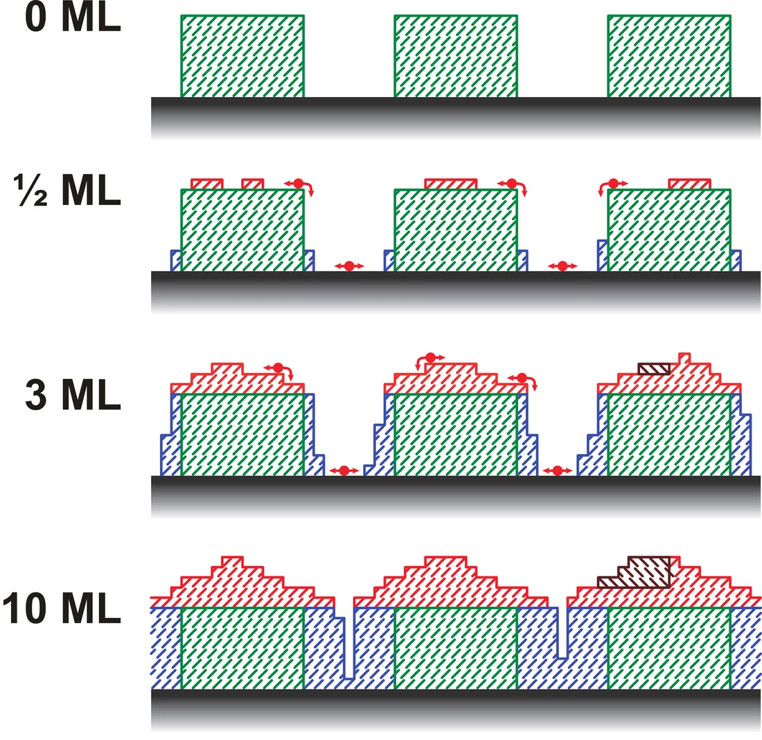
Researchers at IMEC Belgium have developed a double-step method to grow a closed and dense highly crystalline thin film over several square millimetres. The first step is the growth of individual, non-connected single-crystal ribbons from solution by zone-casting, a meniscus-guided coating technique. The second step is the growth of typically ten monolayers of the same organic semiconductor by thermal evaporation. The grown layer is found to be epitaxially templated on the crystal seeds of the ribbons, such that it can be considered homo-epitaxial. Importantly, the molecules landing in the gap between ribbons diffuse to the ribbon edge and condense there, forming a homo-epitaxial layer of several monolayers high that closes cracks, voids, and gaps over distances up to several microns between parallel single-crystalline ribbons present in the initial film. This method is success fully applied to the growth of the small molecule 2,7-dioctyl[1]benzothieno[3,2-b][1]benzothiophene (C8-BTBT). Resulting transistors have much superior characteristics to transistors formed by either evaporated or meniscus-guided crystalline thin-film semi-conductor layers.
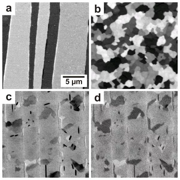
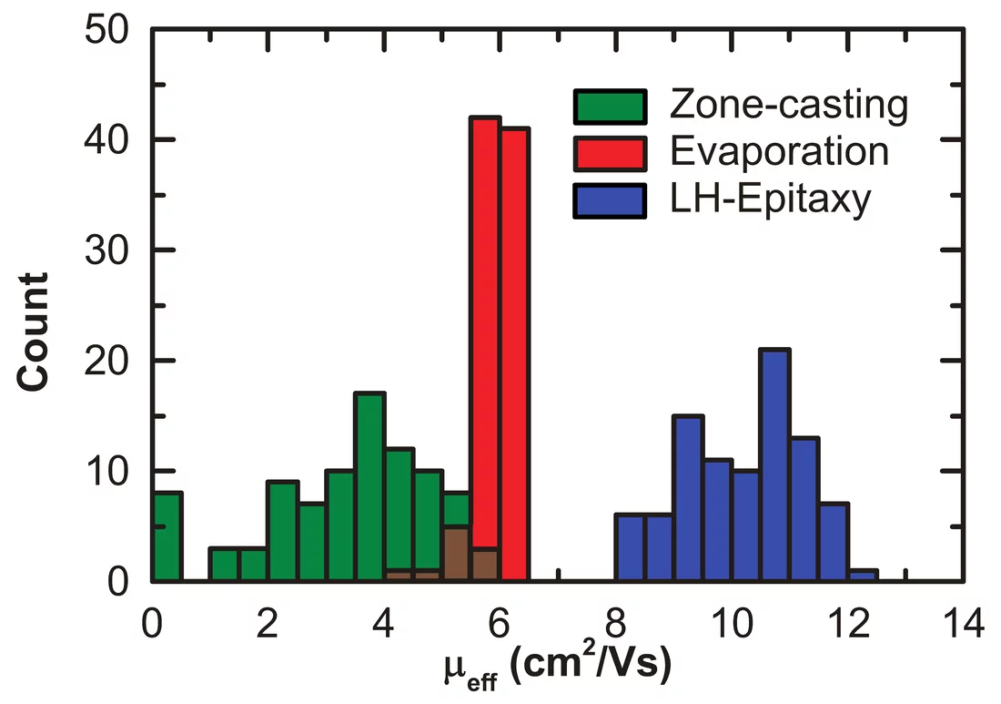
Scanning transmission soft X-ray spectro-microscopy (STXM) was performed at the Swiss Light Source to assess and demonstrate the molecular orientation and crystal domain structure of thin C8-BTBT films fabricated via different methods. By tuning the X-ray energy to the carbon 1s→π* molecular transition, the contrast of the images becomes dependent on the orientation of the molecules via linear dichroism (film thickness effects were removed by dividing by an image measured at a non-dichroic X-ray energy). Thus the orientation of the molecules in each crystalline domain relative to the polarisation axis of the X-ray beam (horizontal) is expressed in the image as a shade of grey. The IMEC double-step process was observed to repair the cracks and defects in the template zone-cast striped films with the overlaying material tending to take on the molecular orientation of the template. More surface-sensitive measurements performed by measuring the photo-emitted electrons revealed that the few observed misoriented domains were restricted to surface layers and hence should not significantly impact electrical performance of the film. Thin film transistors based on these C8-BTBT films deliver excellent electrical characteristics: The average aggregate mobility measured over 90 devices is higher than 10 cm2 V−1 s−1 with a spread of 10%. This is a significant improvement over the performance of zone-cast-only films. Besides, this is the highest aggregate mobility for the commonly used small molecule C8-BTBT. This method should be applicable to other organic semiconductors that are processable both in liquid and vapour phases, and possibly even perovskite materials.
Contact
Dr. Cedric RolinSenior Researcher
IMEC, Large Area Electronics Department
Kapeldreef 75, 3001 Leuven, Belgium
Telephone: +32 16 28 18 74
E-mail: cedric.rolin@imec.be
Dr. Benjamin Watts
PolLux Beamline Scientist
Paul Scherrer Institut
Telephone: +41 56 310 5516
E-mail: benjamin.watts@psi.ch
Original Publication
Highly Crystalline C8-BTBT Thin-Film Transistors by Lateral Homo-Epitaxial Growth on Printed TemplatesRobby Janneck, Nicolas Pilet, Satya Prakash Bommanaboyena, Benjamin Watts, Paul Heremans, Jan Genoe, and Cedric Rolin
Advanced Materials 1703864 (2017)
DOI: 10.1002/adma.201703864


