
Search
3D imaging for planar samples with zooming
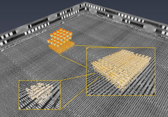
Researchers of the Paul Scherrer Institut have previously generated 3-D images of a commercially available computer chip. This was achieved using a high-resolution tomography method. Now they extended their imaging approach to a so-called laminography geometry to remove the requirement of preparing isolated samples, also enabling imaging at various magnification. For ptychographic X-ray laminography (PyXL) a new instrument was developed and built, and new data reconstruction algorithms were implemented to align the projections and reconstruct a 3D dataset. The new capabilities were demonstrated by imaging a 16 nm FinFET integrated circuit at 18.9 nm 3D resolution at the Swiss Light Source. The results are reported in the latest edition of the journal Nature Electronics. The imaging technique is not limited to integrated circuits, but can be used for high-resolution 3D imaging of flat extended samples. Thus the researchers start now to exploit other areas of science ranging from biology to magnetism.