
In situ stress observation in oxide films and how tensile stress influences oxygen ion conduction
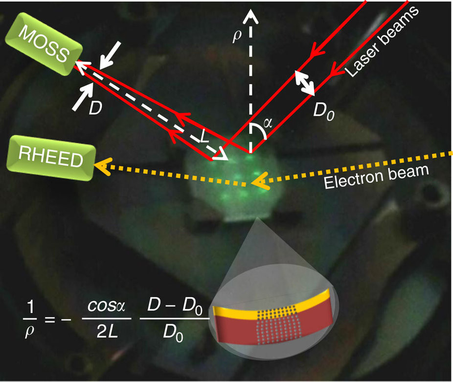
Many properties of materials can be changed by varying the interatomic distances in the crystal lattice by applying stress. Ideal model systems for investigations are heteroepitaxial thin films where lattice distortions can be induced by the crystallographic mismatch with the substrate. Here we describe an in situ simultaneous diagnostic of growth mode and stress during pulsed laser deposition of oxide thin films. The stress state and evolution up to the relaxation onset are monitored during the growth of oxygen ion conducting Ce0.85Sm0.15O2-δ; thin films via optical wafer curvature measurements. Increasing tensile stress lowers the activation energy for charge transport and a thorough characterization of stress and morphology allows quantifying this effect using samples with the conductive properties of single crystals. The combined in situ application of optical deflectometry and electron diffraction provides an invaluable tool for strain engineering in Materials Science to fabricate novel devices with intriguing functionalities.