
Plasmonic Arrays for Sensor Applications
Noble metal nanostructures can support plasmons that have the ability to localize light to subwavelength regions. The strongly amplified electromagnetic field in such regions can be used to locally enhance the excitation of molecules such that ultimately single molecules can be detected.
The main objective of this project is the development of new plasmonic arrays for practical sensing purposes. With the combination of EUV interference lithography and angular metal evaporation, we fabricate a broad range of periodic arrays, from sub-10 nm gap arrays [1,6] to kagome lattices over mm2 large areas. Practical aspects such as excellent signal reproducibility and chip reusability [2] can be achieved that have previously been one of the reasons for unsuccessful commercialization. The underlying enhancement mechanism is studied with 3D surface integral simulations and leads to a detailed understanding of the electromagnetic field localization [3,4].
The main objective of this project is the development of new plasmonic arrays for practical sensing purposes. With the combination of EUV interference lithography and angular metal evaporation, we fabricate a broad range of periodic arrays, from sub-10 nm gap arrays [1,6] to kagome lattices over mm2 large areas. Practical aspects such as excellent signal reproducibility and chip reusability [2] can be achieved that have previously been one of the reasons for unsuccessful commercialization. The underlying enhancement mechanism is studied with 3D surface integral simulations and leads to a detailed understanding of the electromagnetic field localization [3,4].
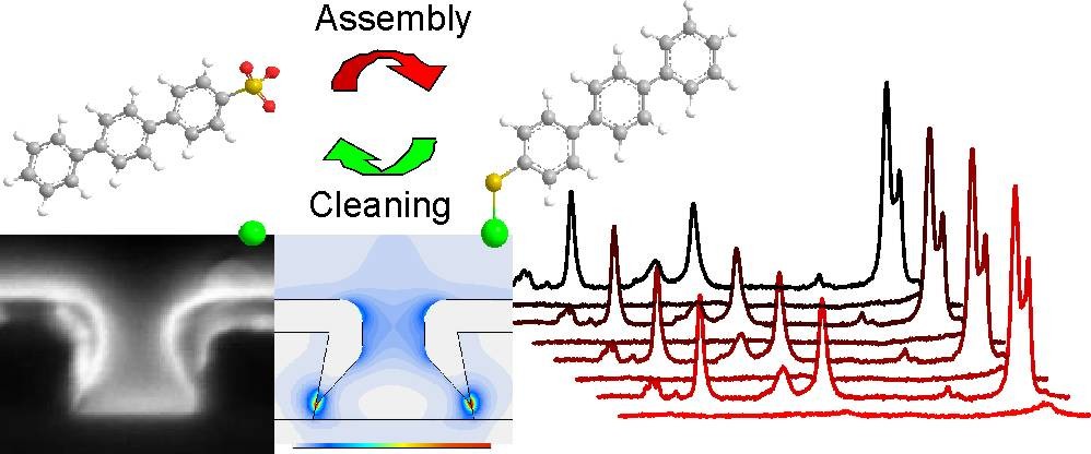
Figure 1: Plasmonic arrays for reusable SERS sensors
Our gap arrays consist of a crescent shaped cross section that supports Fano-resonances sensitive to Ångström changes of the metal displacement. With the measurement of plasmon radiance changes, a novel sensor can be developed with higher sensitivity than resonance shift experiments [4]. Fabrication parameters such as the adhesion layer are engineered to minimize plasmon damping and obtain pattern with highest enhancement factors [5].
Collaboration: O.J.F. Martin, EPFL Funding: SNF 124777
Thesis: Thomas Siegfried: Near field Enhancement in Plasmonic Arrays, EPFL, Lausanne 2014. DOI:10.5075/epfl-thesis-6114
Collaboration: O.J.F. Martin, EPFL Funding: SNF 124777
Thesis: Thomas Siegfried: Near field Enhancement in Plasmonic Arrays, EPFL, Lausanne 2014. DOI:10.5075/epfl-thesis-6114
References
[1] T. Siegfried, Y. Ekinci, H. H. Solak, O. J. F. Martin, and H. Sigg, Appl. Phys. Lett. (2011), 99, 263302. DOI:10.1063/1.3672045
[2] T. Siegfried, M. Kind, A. Terfort, O. J. F. Martin, M. Zharnikov, N. Ballav, H. Sigg, Journal of Raman Spectroscopy (2012). DOI:10.1002/jrs.4163
[3] B. Gallinet, A. Lovera, T. Siegfried, H. Sigg, O. J. F. Martin, AIP Conf. Proc. (2012), 1475, 18-20. DOI:10.1063/1.4750081
[4] B. Gallinet, T. Siegfried, H. Sigg, P. Nordlander, O. J. F. Martin, Nano Letters (2013), 13 (2), pp 497–503. DOI:10.1021/nl303896d
[5] T. Siegfried, Y. Ekinci, O. J. F. Martin, H. Sigg, ACS Nano (2013), 7 ( 3), 2751– 2757. DOI:10.1021/nn4002006
[6] T. Siegfried, Y. Ekinci, O. J. F. Martin, H. Sigg, Nano Letters (2013), 13 (11), 5449-5453. DOI:10.1021/nl403030g