
Scientific Highlights 2013
Magnetismus im Stress: Gleichzeitiger Anti- und Ferromagnetismus
Abstract: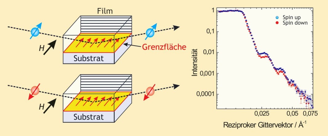
Polarisierte Neutronen beider Spinausrichtungen up (blau) und down (rot) gelangen unter sehr kleinen Einfallswinkeln in eine Probe. Dort werden sie an den im Magnetfeld H ausgerichteten Momenten gestreut, hier dargestellt für eine Grenzfläche. Aus den gemessenen Unterschieden der Winkelabhängigkeit für beide Spinrichtungen lässt sich ein magnetisches Tiefenprofil ableiten.
Die gleichzeitige Existenz von Magnetismus und Ferroelektrizät in einem Material ist selten. Setzt sich dieser Magnetismus aus mehreren unabhängigen, magnetischen Grundzuständen zusammen, ist das ungewöhnlich. Einer schweizerisch-französischen Zusammenarbeit unter Leitung des Paul Scherrer Instituts ist es gelungen, mehrere magnetische Grundzustände in einem Material zu realisieren und detailliert zu untersuchen.
Applications of laser printing for organic electronics
Abstract:
The development of organic electronic requires a non contact digital printing process. The European funded e-LIFT project investigated the possibility of using the Laser Induced Forward Transfer (LIFT) technique to address this field of applications. This process has been optimized for the deposition of functional organic and inorganic materials in liquid and solid phase, and a set of polymer dynamic release layer (DRL) has been developed to allow a safe transfer of a large range of thin films. Then, some specific applications related to the development of heterogeneous integration in organic electronics have been addressed. We demonstrated the ability of LIFT process to print thin film of organic semiconductor and to realize Organic Thin Film Transistors (OTFT) with mobilities as high as 4 10-2 cm2.V-1.s-1 and Ion/Ioff ratio of 2.8 105. Polymer Light Emitting Diodes (PLED) have been laser printed by transferring in a single step process a stack of thin films, leading to the fabrication of red, blue green PLEDs with luminance ranging from 145 cd.m-2 to 540 cd.m-2. Then, chemical sensors and biosensors have been fabricated by printing polymers and proteins on Surface Acoustic Wave (SAW) devices. The ability of LIFT to transfer several sensing elements on a same device with high resolution allows improving the selectivity of these sensors and biosensors. Gas sensors based on the deposition of semiconducting oxide (SnO2) and biosensors for the detection of herbicides relying on the printing of proteins have also been realized and their performances overcome those of commercial devices. At last, we successfully laser-printed thermoelectric materials and realized microgenerators for energy harvesting applications.
Interface superconductor with gap behaviour like a high-temperature superconductor
Abstract:
Photograph (a) and schematic cross section (b) of a typical Au–LaAlO3–SrTiO3 tunnel device. The broad gold ring (inner diameter, 160 μm) lies on top of the LaAlO3 layer, which serves as a tunnel barrier between the 2DEL and the Au. The outer ring and the centre contact of the device are Au-covered Ti contacts to the 2DEL. c, Cross-sectional high-angle annular dark-field STEM image of a Au–LaAlO3–SrTiO3 tunnel junction. The image is taken along the zone axis of the perovskite unit cells. a.u., arbitrary units.
The physics of the superconducting state in two-dimensional (2D) electron systems is relevant to understanding the high-transition-temperature copper oxide superconductors and for the development of future superconductors based on interface electron systems. But it is not yet understood how fundamental superconducting parameters, such as the spectral density of states, change when these superconducting electron systems are depleted of charge carriers. Here we use tunnel spectroscopy with planar junctions to measure the behaviour of the electronic spectral density of states as a function of carrier density, clarifying this issue experimentally. We chose the conducting LaAlO3–SrTiO3 interface as the 2D superconductor, because this electron system can be tuned continuously with an electric gate field3. We observed an energy gap of the order of 40 microelectronvolts in the density of states, whose shape is well described by the Bardeen–Cooper–Schrieffer superconducting gap function. In contrast to the dome-shaped dependence of the critical temperature, the gap increases with charge carrier depletion in both the underdoped region and the overdoped region. These results are analogous to the pseudogap behaviour of the high-transition-temperature copper oxide superconductors and imply that the smooth continuation of the superconducting gap into pseudogap-like behaviour could be a general property of 2D superconductivity.
Strain-Induced Ferromagnetism in Antiferromagnetic LuMnO3 Thin Films
Abstract:
Diagram of the processes in the LuMnO3 layers studied. The layer is highly strained close to the substrate, which leads to a ferromagnetic (FM) order there. As the distance grows, the strain decreases so that two antiferromagnetic (AFM) orders appear: the spin spirals and the E-type, where two spins point in one direction and the next two in the other.
Single phase and strained LuMnO3 thin films are discovered to display coexisting ferromagnetic and antiferromagnetic orders. A large moment ferromagnetism (≈1μB), which is absent in bulk samples, is shown to display a magnetic moment distribution that is peaked at the highly strained substrate-film interface. We further show that the strain-induced ferromagnetism and the antiferromagnetic order are coupled via an exchange field, therefore demonstrating strained rare-earth manganite thin films as promising candidate systems for new multifunctional devices.
Electric-Field-Induced Polar Order and Localization of the Confined Electrons in LaAlO3/SrTiO3 Heterostructures
Abstract: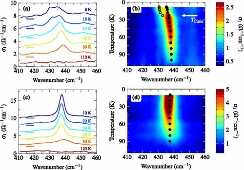
(a), (b) IR spectra showing the T dependence of the R mode in a SrTi18O3 single crystal with a ferroelectric transition at TCurie=23 K. (c), (d) Corresponding spectra of quantum paraelectric SrTi16O3.
With ellipsometry, x-ray diffraction, and resistance measurements we investigated the electric-field effect on the confined electrons at the LaAlO3/SrTiO3 interface. We obtained evidence that the localization of the electrons at negative gate voltage is induced, or at least enhanced, by a polar phase transition in SrTiO3 which strongly reduces the lattice polarizability and the subsequent screening. In particular, we show that the charge localization and the polar order of SrTiO3 both develop below ∼50 K and exhibit similar, unipolar hysteresis loops as a function of the gate voltage.
On Proton Conductivity in Porous and Dense Yttria Stabilized Zirconia at Low Temperature
Abstract: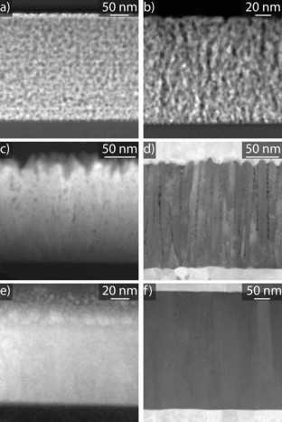
HAADF STEM micrographs of YSZ thin films deposited by different methods. a) 8YSZ SP (Tdep = 370 °C; Tpa = 600 °C, 20 h), b) 8YSZ AA-CVD (Tdep = 450 °C, Tpa = 600 °C, 20 h), c) 8YSZ AA-CVD (Tdep = 600 °C, Tpa = 600 °C for 20 h), d) 3YSZ PLD (Tdep = 450 °C, pO2 = 7 Pa, Tpa = 600 °C, 1 h) with top and bottom electrode, e) 3YSZ PLD (Tdep = 450 °C, pO2 = 1 Pa, Tpa = 600 °C, 1 h), and f) 8YSZ PLD (Tdep = 700 °C, pO2 = 2.7 Pa, Tpa = 600 °C, 20 h) with top and bottom electrodes.
The electrical conductivity of dense and nanoporous zirconia-based thin films is compared to results obtained on bulk yttria stabilized zirconia (YSZ) ceramics. Different thin film preparation methods are used in order to vary grain size, grain shape, and porosity of the thin films. In porous films, a rather high conductivity is found at room temperature which decreases with increasing temperature to 120 °C. This conductivity is attributed to proton conduction along physisorbed water (Grotthuss mechanism) at the inner surfaces. It is highly dependent on the humidity of the surrounding atmosphere. At temperatures above 120 °C, the conductivity is thermally activated with activation energies between 0.4 and 1.1 eV. In this temperature regime the conduction is due to oxygen ions as well as protons. Proton conduction is caused by hydroxyl groups at the inner surface of the porous films. The effect vanishes above 400 °C, and pure oxygen ion conductivity with an activation energy of 0.9 to 1.3 eV prevails. The same behavior can also be observed in nanoporous bulk ceramic YSZ. In contrast to the nanoporous YSZ, fully dense nanocrystalline thin films only show oxygen ion conductivity, even down to 70 °C with an expected activation energy of 1.0 ± 0.1 eV. No proton conductivity through grain boundaries could be detected in these nanocrystalline, but dense thin films.
The fabrication of small molecule organic light-emitting diode pixels by laser-induced forward transfer
Abstract: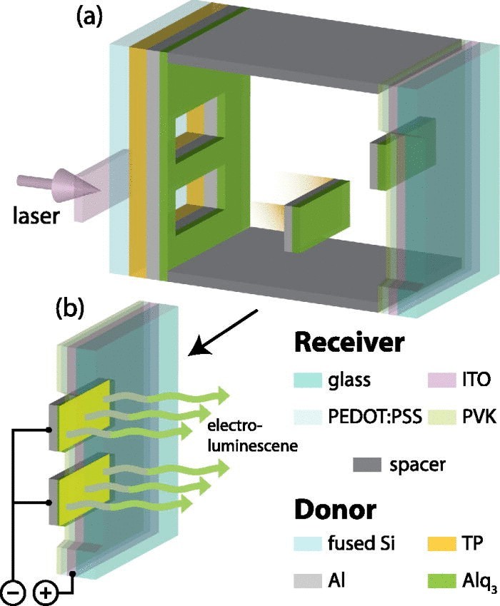
A scheme showing the LIFT process. The laser beam punching out an Alq3 pixel for transfer from the donor to the receiver substrate is shown in (a), and pair of electroluminescent pixels are shown with a bias applied in(b).
Laser-induced forward transfer (LIFT) is a versatile organic light-emitting diode (OLED) pixel deposition process, but has hitherto been applied exclusively to polymeric materials. Here, a modified LIFT process has been used to fabricate small molecule Alq3 organic light-emitting diodes (SMOLEDs). Small molecule thin films are considerably more mechanically brittle than polymeric thin films, which posed significant challenges for LIFT of these materials. The LIFT process presented here uses a polymeric dynamic release layer, a reduced environmental pressure, and a well-defined receiver-donor gap. The Alq3 pixels demonstrate good morphology and functionality, even when compared to conventionally fabricated OLEDs. The Alq3 SMOLED pixel performances show a significant amount of fluence dependence, not observed with polymerical OLED pixels made in previous studies. A layer of tetrabutyl ammonium hydroxide has been deposited on top of the aluminium cathode, as part of the donor substrate, to improve electron injection to the Alq3, by over 600%. These results demonstrate that this variant of LIFT is applicable for the deposition of functional small molecule OLEDs as well as polymeric OLEDs.